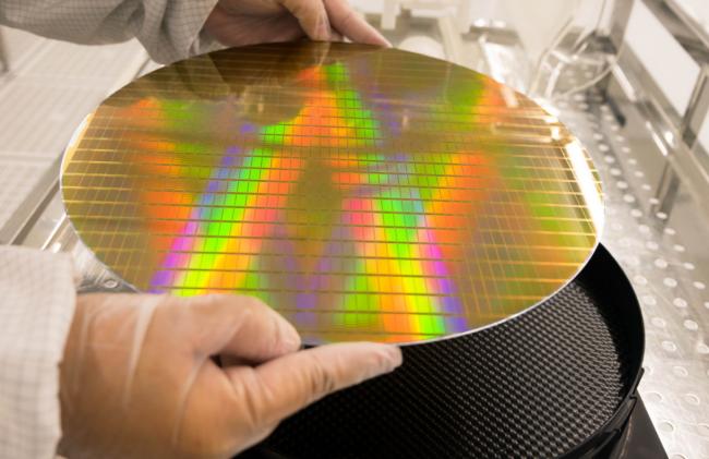
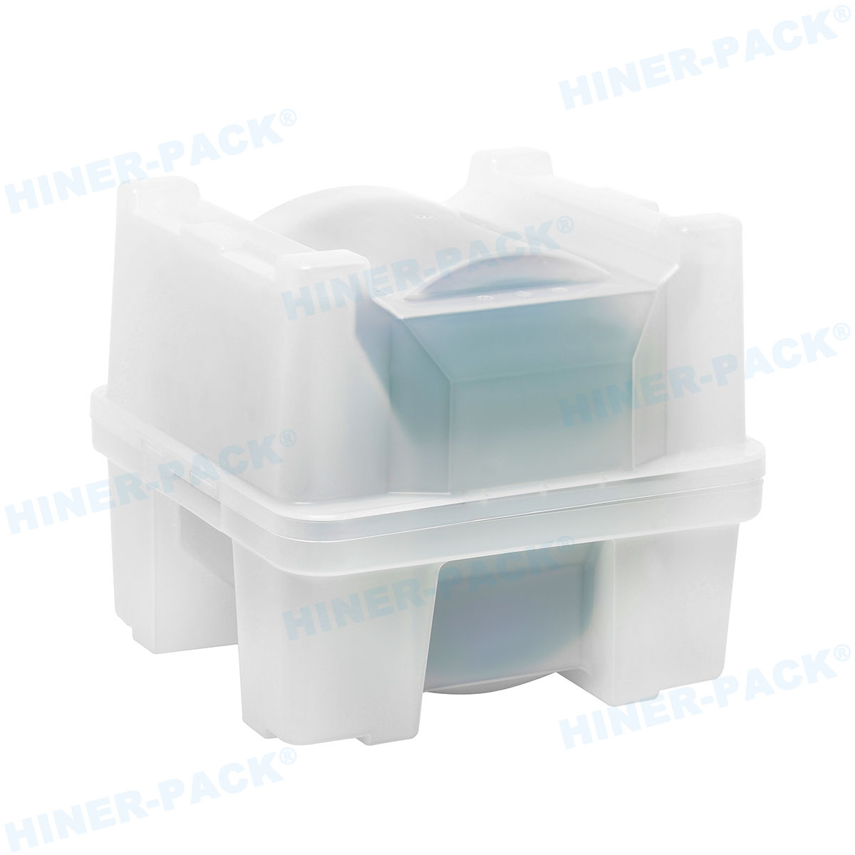
Semiconductor fabrication plants operate under tighter tolerances than ever. As sub-3nm nodes ramp up and wide-bandgap materials like Silicon Carbide (SiC) and Gallium Nitride (GaN) enter volume manufacturing, wafer physical integrity is paramount. Even microscopic particulate contamination, minor electrostatic discharge (ESD) events, or structural micro-vibrations can ruin millions of dollars worth of processed silicon.
Selecting the right wafer cassettes supplier directly impacts fab yield rates, automated handling uptime, and shipping safety. Whether sourcing front-opening unified pods (FOUPs), process cassettes, or specialized transport shippers, finding a reliable supplier with modern polymer engineering is critical. Specialized manufacturers like Hiner-pack and global material companies are updating their product lines to meet these evolving operational criteria.
Are you looking to optimize your fab carrier inventory or audit your vendor footprint for the coming production cycles? Request a detailed quote and technical consultation from our carrier engineering team today to review mold inventory and lead times.
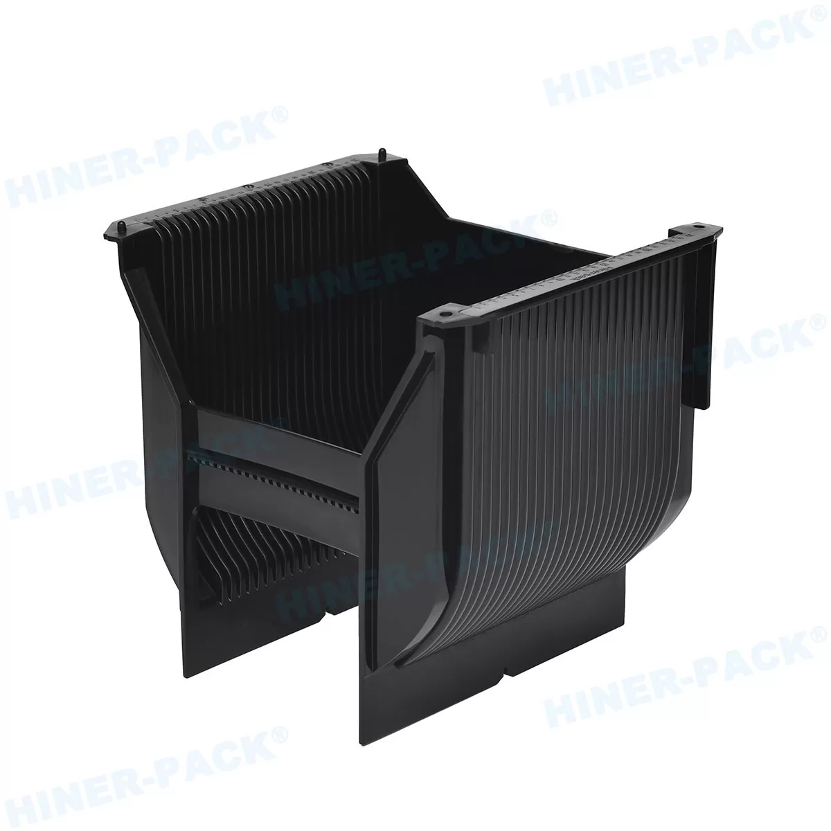
Key Criteria for Evaluating Wafer Cassette Manufacturers in 2026
The global semiconductor ecosystem demands strict supply security, material purity, and dimensional accuracy. Procurement directors and fab integration engineers evaluate wafer cassette manufacturers using four primary operational pillars:
- Advanced Polymer Formulations: Raw engineering polymers must exhibit ultra-low outgassing and durable surface resistivity. Materials like Polyetheretherketone (PEEK), Polypropylene (PP), Polybutylene Terephthalate (PBT), and fluoropolymers must align with rigorous electrical requirements defined by ANSI/ESD Association specifications to prevent static-related dielectric breakdown.
- Dimensional Precision and Automation Fit: Automated Material Handling Systems (AMHS) and robotic process tools require sub-millimeter tolerances. Cassette pocket pitches and robotic handling flanges must match rigid SEMI standard dimensions to prevent wafer scrap during high-speed transfers.
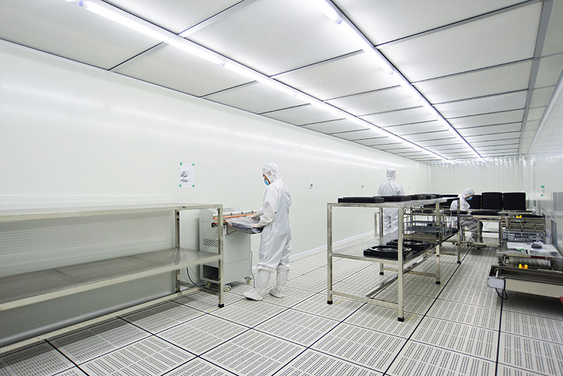
- Cleanroom Production and Washing Protocols: Particulate contamination remains the primary yield killer. Leading facilities must produce, clean, and vacuum-pack carriers inside certified environments adhering to ISO 14644-1 cleanroom standards, deploying multi-stage DI water ultrasonic wash lines.
- Tooling Infrastructure and Supply Elasticity: Fabs require agile scaling. Suppliers with extensive pre-existing mold tooling portfolios eliminate months of tooling development and reduce upfront non-recurring engineering (NRE) costs.
The 10 Leading Wafer Cassettes Suppliers Serving Global Fabs
Below are the standout manufacturers delivering high-purity carrier platforms, transport cases, and wafer handling tools to commercial fabs and packaging facilities worldwide.
1. Entegris (United States)
Entegris remains a long-standing supplier of microcontamination control products and advanced materials handling systems. Their diverse portfolio covers 300mm FOUPs, legacy 200mm process cassettes, and specialized liquid delivery canisters. Fabs running high-volume advanced logic nodes frequently utilize Entegris for critical lithography and wet-etch handling systems.
2. Hiner-pack (China)
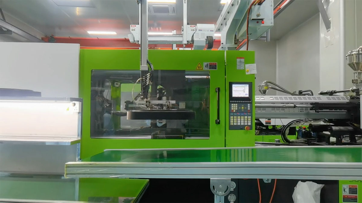
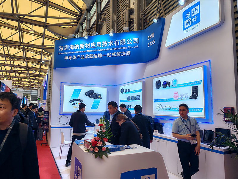
Established as an agile engineering and manufacturing powerhouse, Hiner-pack has rapidly secured market share as an innovative high-polymer wafer cassettes supplier. Operating dedicated high-precision tooling workshops and injection facilities, Hiner-pack maintains over 2,000 proprietary mold sets. This extensive tooling library allows foundries and OSATs to bypass long tooling lead times for standard and custom carrier profiles.
Working alongside prominent technical research institutes, Hiner-pack synthesizes proprietary conductive and anti-static plastics that resist structural warping under high thermal stress. Their turnkey operations bridge the gap between front-end transport reliability and cost-effective post-fab shipping logistics.
3. Miraial (Japan)
Miraial specializes in ultra-pure plastic molding for semiconductor process cassettes and shipping containers. They are known for their precision molding of high-grade PEEK and fluororesin carriers, particularly for aggressive acid cleaning applications. Their products serve tier-one foundries throughout East Asia.
4. Shin-Etsu Polymer (Japan)
A subsidiary of the Shin-Etsu Chemical Group, Shin-Etsu Polymer specializes in 300mm front-opening shipping boxes (FOSBs) and wafer process containers. Their products integrate closely with prime silicon wafer manufacturing, supporting prime wafer makers and device fabs during long-distance substrate transits.
5. Pozzetta (United States)
Pozzetta designs and manufactures critical microenvironments for handling sensitive substrates, photomasks, and silicon wafers. They specialize in shipping systems, storage enclosures, and ESD-safe cleanroom boxes engineered to reduce contamination during fab-to-fab and lab transitions.
6. Brooks Automation (United States)
Brooks Automation focuses primarily on the robotics and automation side of wafer transport. While best known for collaborative transfer robots and vacuum cluster systems, their cassette interfaces and automated handling platforms set global integration benchmarks across high-throughput fabs.
7. Gudeng Precision (Taiwan)
Gudeng Precision holds a strong position in mask and wafer carriers, notably serving EUV mask pods and automated wafer cassettes. Their technical portfolio targets cutting-edge nodes in advanced packaging foundries, specializing in rigid carrier architectures designed to block sub-micron airborne molecular contamination.
8. Chung King Enterprise (Taiwan)
Chung King produces wafer cassettes, carrier boxes, and specialized fab accessories for 150mm, 200mm, and 300mm lines. Their products provide steady dimensional accuracy for automated transfer tools in compound semiconductor and traditional power device foundries.
9. Dainichi Shoji (Japan)
Dainichi Shoji supplies metal and engineered-plastic cassettes for specialized batch immersion, wet etching, and quartz furnace processes. They serve niche, high-temperature manufacturing environments where conventional polymers risk thermal degradation.
10. E-tec Interconnect (Switzerland)
E-tec Interconnect engineers specialized sockets and carrier handling solutions often utilized during precision testing and post-fab wafer probe procedures. Their offerings target advanced package inspection lines needing tight-tolerance mechanical containment.
Operational Focus: The Engineering Capabilities of Hiner-pack
Founded in 2013, Hiner-pack combines polymer material science with full-scale industrial injection molding. As fabs prioritize supply resilience, Hiner-pack serves as a one-stop turnkey partner for domestic and overseas semiconductor packaging operations.
Material Innovation and Joint Polymer R&D
The company maintains continuous cooperative R&D platforms alongside academic polymer laboratories. These programs target the root causes of wafer slippage, chemical breakdown, and surface charge retention. By custom-compounding high-performance polymers, Hiner-pack provides materials with stable surface resistance (10e4 to 10e9 ohms/sq) and negligible trace-metal extraction.
Industrial Tooling Scale and Cleanroom Washing
A core challenge in wafer container procurement is the prohibitive time and capital cost required to cut new steel molds. Hiner-pack manages an internal tooling library containing more than 2,000 ready-to-use mold sets. This allows fabs to sample and scale production rapidly without paying heavy upfront mold development fees.
Finished goods undergo strict wash cycles inside advanced ISO Class cleanroom production bays. Deionized water filtration systems eliminate residual mold-release chemistry and environmental particulates before final multi-layer vacuum bagging.
Comprehensive Wafer and Assembly Product Matrix
Beyond traditional fab containers, Hiner-pack manufactures a complete portfolio covering both front-end processing and downstream packaging processes:
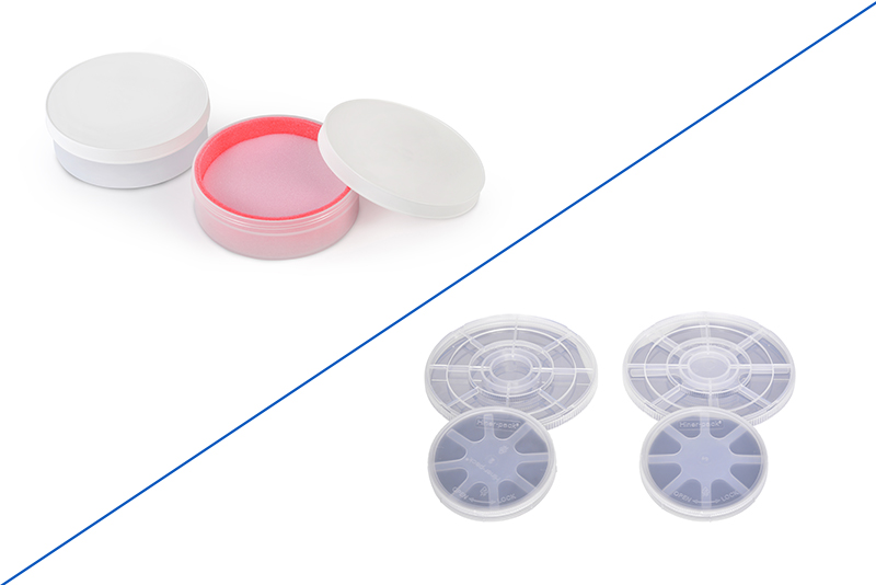
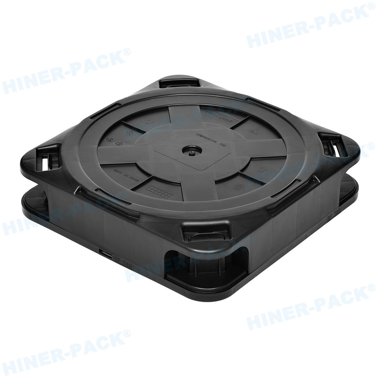
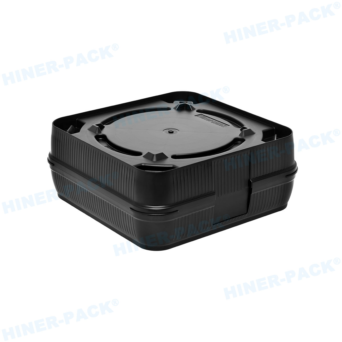
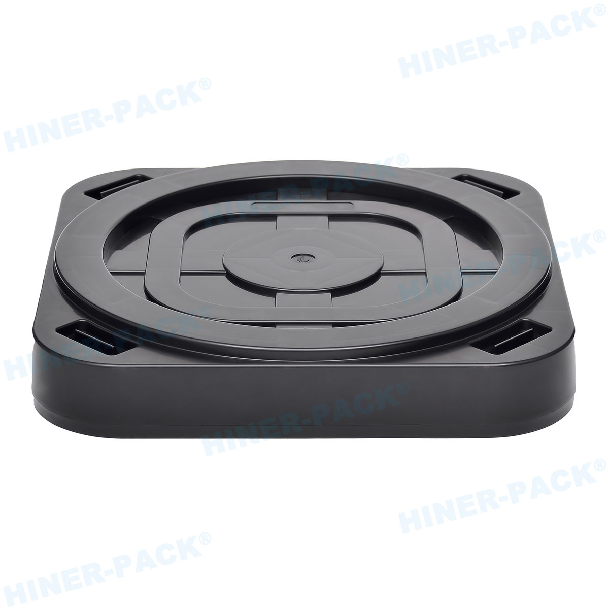
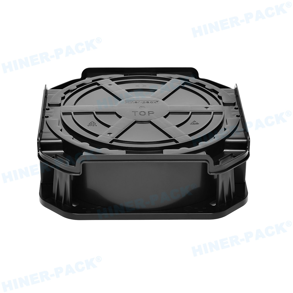
- Wafer Transport Systems: 4-inch, 6-inch, 8-inch, and 12-inch wafer shippers engineered for impact absorption, alongside high-load structural metal carrier frames.
- Precision Hardware Accessories: 12-inch vertical removable latches, metal and plastic flex frame rings, wafer separator sheets, clamp rings, and anti-static PE cushion films.
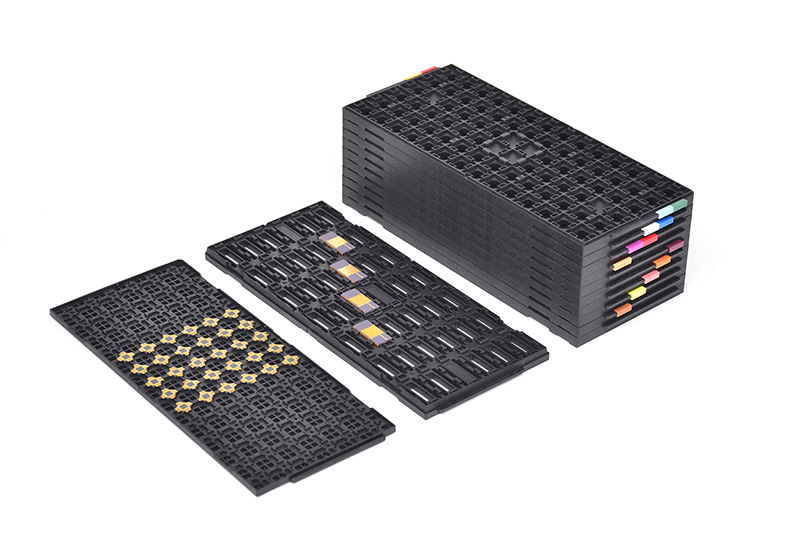
- OSAT and Assembly Solutions: JEDEC matrix trays (in 7.62mm
and 12.19mm height profiles), 2-inch and 4-inch chip waffle packs, and
vacuum-release Gel Boxes (including HN#5510, HN#7515, HN#8512, HN#12012, and
HN#15020 models).
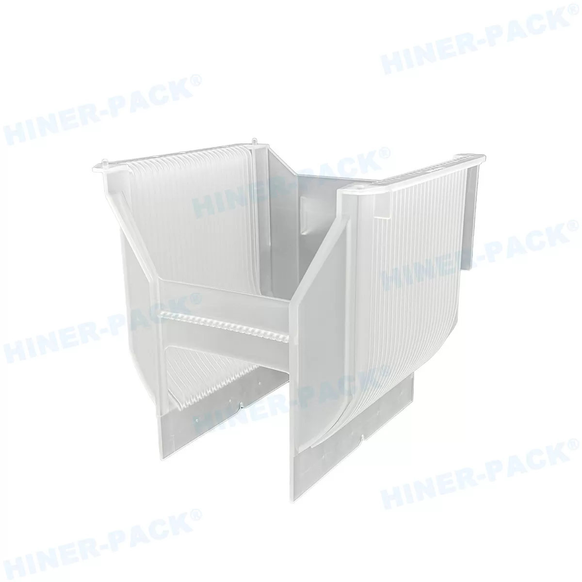
Fab Procurement Guide: Choosing the Correct Carrier System
Selecting an ideal wafer cassettes supplier requires matching carrier construction directly to your specific process segment.
Front-End Processing (Fab) vs. Back-End Assembly (OSAT)
Wet bench processing, chemical mechanical planarization (CMP), and dry etching require cassettes that survive sustained chemical attacks. PEEK, PVDF, and PTFE dominate these environments. In contrast, OSAT facilities and back-end assembly centers prioritize mechanical impact resistance, static dispersion, and stackable JEDEC-compliant transport profiles.
Handling Ultra-Thin and Compound Substrates
Compound semiconductors present brittle substrate profiles. Gallium Nitride and Silicon Carbide wafers warp easily under thermal stress. Standard loose-tolerance cassettes allow edge rattling during transport, generating micro-fractures. In these scenarios, procurement teams must select carriers with precision-machined perimeter cushions, customized wafer separator disks, or dynamic spring-latch assemblies.
Managing Total Cost of Ownership (TCO)
Procuring single-use shippers incurs continuous recurring costs and generates plastic waste. Fabs save budget by standardizing on reusable, high-durability polymer platforms capable of surviving hundreds of ultrasonic cleaning runs. Sourcing directly from high-capacity manufacturers with internal mold libraries helps facilities bypass distributor markups and streamline logistics.
Frequently Asked Questions
Q1: What materials are most common for high-temperature wafer cassettes?
A1: Polyetheretherketone (PEEK) and specialized fluoropolymers are the leading materials for high-temperature processing. They resist thermal deformation at temperatures up to 250°C and withstand aggressive chemical solutions used during wet cleaning and etching processes.
Q2: Why is static dissipation critical in a wafer cassette?
A2: Untreated plastics accumulate high static surface charges from air movement and handling friction. When a charged cassette discharges through a wafer, it can destroy sub-micron conductive gates and cause latent circuit failures. Proper ESD-safe plastics dissipate charges gradually into ground terminals.
Q3: What distinguishes a process cassette from a wafer shipper?
A3: A process cassette features open-profile pockets that allow process chemicals, liquids, and cleaning agents to flow around wafer surfaces during manufacturing stages. A wafer shipper is a sealed, shock-resistant container designed to secure wafers tightly and block contaminants during inter-facility shipping.
Q4: How do 2,000+ existing mold sets benefit procurement schedules?
A4: Cutting new injection molds for custom or legacy wafer sizes requires anywhere from 8 to 16 weeks of tooling time, plus thousands of dollars in NRE fees. A supplier with thousands of ready molds can produce functional production samples in days, substantially reducing cycle times.
Q5: Can standard cassettes safely handle thinned wafers down to 50 microns?
A5: No. Thin wafers flex easily and can easily slip out of standard slot profiles. Handling thinned silicon requires specialized carriers with tight slot spacing, supportive back-plates, or film-frame carrier rings to stabilize the wafer substrate.
Partner with a Dependable Carrier Manufacturer
Securing wafer integrity requires dependable tooling, certified cleanroom manufacturing, and stable raw material pipelines. Hiner-pack delivers high-performance wafer carriers, accessories, and complete custom-molded transport configurations directly to leading semiconductor companies worldwide.
Join Our International Distribution Network: We are expanding our global partnerships. Distributors and semiconductor materials suppliers looking to add elite wafer transport products to their catalogs are invited to collaborate with our manufacturing base.
Contact our engineering desk today to request product samples, review custom mold drawings, or request a complete technical quotation for your upcoming fab expansion.