
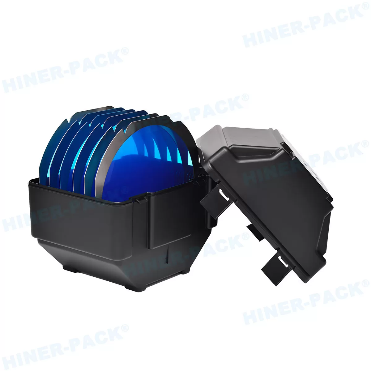
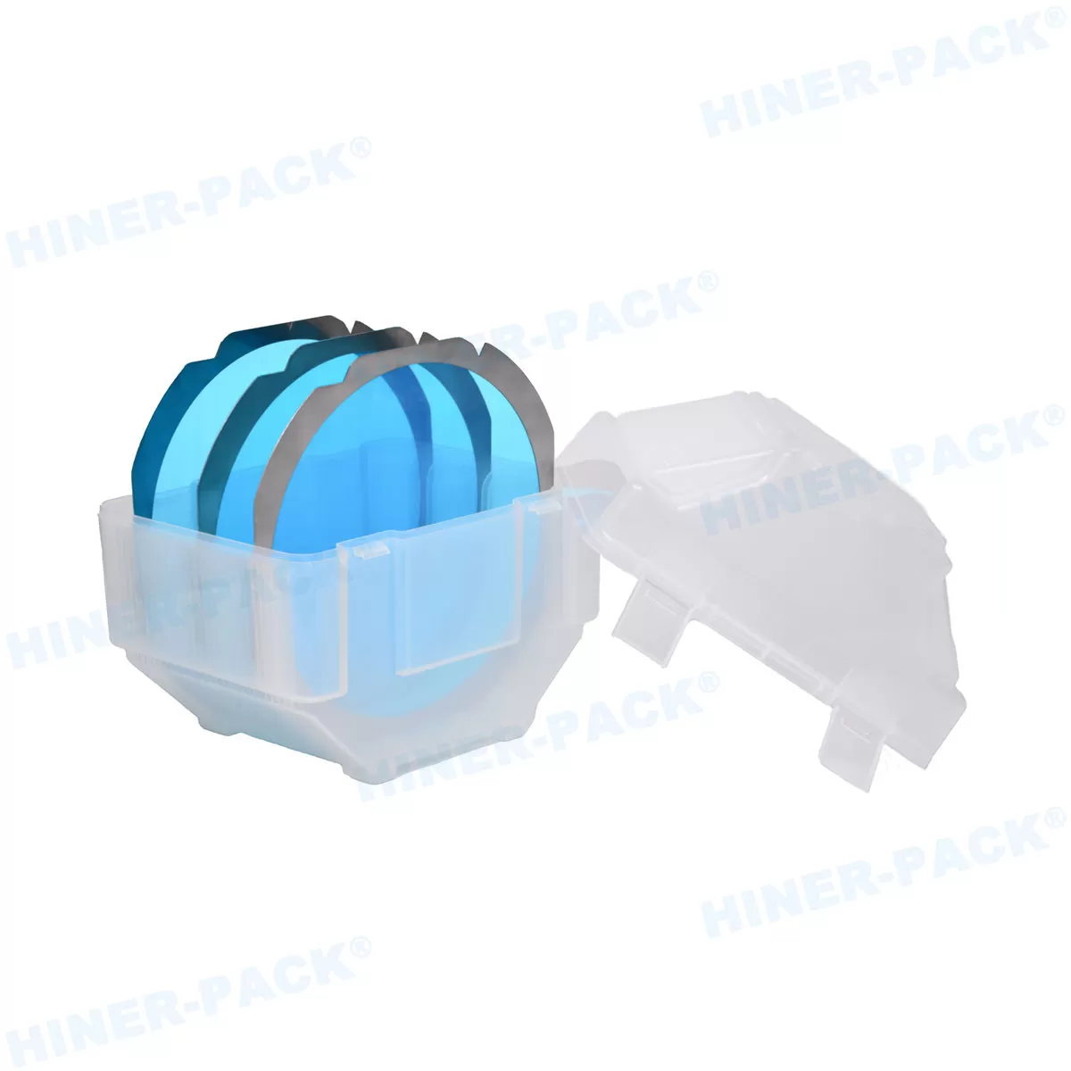
Qualifying an authentic semiconductor wafer holders factory requires evaluating physical manufacturing assets, precision mold maintenance, and contamination control—not superficial trading brochures. In automated fab lines and advanced OSAT facilities, sub-standard carriers lead to robotic transfer jams, particle shedding, and electrostatic die destruction. Founded in 2013, Hiner-pack is a national high-tech manufacturing enterprise operating in-house mold processing, cleanroom injection molding, and certified ultrasonic DI water washing lines. Backed by over 2,000 active mold toolsets and university-partnered polymer laboratories, Hiner-pack directly manufactures full-chain semiconductor carriers—spanning the Wafer Carrier Series, Wafer Shipper Accessories, JEDEC Trays, Waffle Packs / Chip Trays, and Gel Boxes / Vacuum Release Boxes—delivering factory-direct pricing and guaranteed SEMI compliance to global fabs.
An authentic wafer holders factory must possess direct ownership of three operational facilities: in-house CNC and mirror EDM mold machining, all-electric multi-cavity injection presses, and certified ISO Class 4 cleanroom ultrasonic washing lines with 18.2 MΩ·cm hot DI water cascades. Hiner-pack eliminates trading broker markups and waives $3,000–$15,000 NRE mold fees across over 2,000 active mold assets, supplying SEMI-compliant wafer carriers, JEDEC trays, waffle packs, and vacuum release boxes with 72-hour sampling and full batch lot traceability.
Direct manufacturing covering wafer cassettes, shipping accessories, JEDEC baking trays, waffle packs, and gel boxes.
Massive in-house tooling library eliminating tooling fees and compressing standard qualification sampling to 72 hours.
18.2 MΩ·cm hot DI water cascade washing ensures every carrier arrives certified ready for direct fab introduction.
University-partnered polymer compounding locks resistivity at 106–109 Ω/sq with zero particle shedding.
1. Direct Tooling Scale: How 2,000+ Molds Protect Your Capex and Lead Times
Developing custom injection molds for semiconductor carriers introduces severe friction: $5,000 to $20,000 in Non-Recurring Engineering (NRE) fees and 8 to 12 weeks of tooling lead time. Hiner-pack eliminates this barrier through an existing catalog of over 2,000 active mold toolsets, enabling immediate mass production.
When an automated Equipment Front End Module (EFEM) or high-speed die-bonder interacts with a carrier, dimensional consistency is vital. A pocket variance of just 0.05 mm in a JEDEC tray or wafer cassette can misalign robotic vacuum wands, causing edge chipping, bent leads, or dropped wafers.
Complying with international dimensional and handling specifications established by SEMI automated carrier standards and JEDEC packaging design guidelines, Hiner-pack’s manufacturing center controls every production stage:
Zero NRE Tooling Architecture
Our extensive library of over 2,000 active mold toolsets allows global procurement teams to match standard wafer carriers, JEDEC matrix trays, and chip waffle packs with $0 NRE tooling fees and immediate production scheduling.
All-Electric Press Control
Computerized multi-zone cavity pressure control prevents internal shear stress and differential cooling, eliminating long-term thermal warpage across high-temperature baking trays.
18.2 MΩ·cm Hot DI Cascade
Automated multi-stage ultrasonic scrubbing followed by high-resistivity deionized water cascading inside verified ISO Class 4/5 cleanrooms strips all sub-micron debris and chemical residues.
2. Material Science: University-Partnered Polymer R&D and Permanent ESD Protection
A precision wafer holder must prevent electrostatic discharge (ESD) events while eliminating particulate generation. As a pioneer of R&D in semiconductor carrier products, Hiner-pack partners with domestic universities and research institutes to synthesize proprietary conductive polymers that disperse static charges safely without ionic leaching.
Low-tier plastic carriers rely on temporary surface surfactants that evaporate, wash off during wet cleaning, and outgas volatile organic compounds (VOCs) that condense onto exposed copper interconnects. Other manufacturers load standard polymers with excessive raw carbon powder, which sloughs off under friction to create catastrophic conductive particle clouds.
Conforming to electrostatic discharge thresholds certified by ANSI/ESD S20.20 static control guidelines and volatile mass screening governed by ASTM E595 outgassing standards, Hiner-pack’s material engineers formulate specialized compound matrixes:
Permanent Matrix Conductivity vs. Topical Surfactants
Hiner-pack blends conductive carbon networks and inherently dissipative polymers directly into the base resin matrix (mPPO, PEEK, PFA, PP, ABS). This locks surface resistivity permanently at 106 to 109 Ω/sq. It remains completely independent of atmospheric humidity, resists acid bath washdowns, and generates zero carbon sloughing across high-density wafer handling.
3. Factory Floor Audit: Checklist Before Placing an Order
4. Factory Quality Protocol: The Hiner-pack 6-Step Lot Acceptance Grid
To ensure zero-defect integration into automated semiconductor packaging lines, Hiner-pack executes a strict 6-stage qualification loop across every production lot, linking raw polymer synthesis directly to coordinate metrology and particle certification.
ICP-MS Trace Metal Analysis
Screening raw polymer compounds to confirm mobile ions (Na, K, Fe, Cu) remain below parts-per-billion thresholds.
Cavity Pressure Control
Multi-zone temperature profiling preventing internal shear stress, flash burrs, and differential cooling warpage.
Full-Axis Optical Coordinate Scan
Automated tactile and optical CMM scanning confirming slot pitch parallelism and pocket dimensions within ±0.05 mm.
Multi-Point Surface Resistivity
Verifying permanent conductive/dissipative surface resistance (106–109 Ω/sq) across pocket roots, sidewalls, and rails.
Ultrasonic Cleanroom Cascade
Continuous multi-bath ultrasonic stripping and 18.2 MΩ·cm hot DI water cascade inside ISO 14644-1 cleanrooms.
Double Vacuum Packaging
Bake-dry dehumidification followed by antistatic vacuum sealing with lot traceability barcoding.
Frequently Asked Questions: Sourcing from a Wafer Holders Factory
What product lines are manufactured directly at Hiner-pack's factory?
A1: Hiner-pack manufactures five core semiconductor packaging and carrying lines directly in-house: (1) Wafer Carrier Series including automated cassettes and horizontal/vertical process boats, (2) Wafer Shipper Accessories including spider springs, cushions, and separators, (3) JEDEC Trays / IC Trays for BGA/QFP packaging and high-temp baking, (4) Waffle Packs / Chip Trays for bare die and optical components, and (5) Gel Boxes / Vacuum Release Boxes for ultra-thin fragile devices.
How does Hiner-pack eliminate NRE tooling charges for new wafer holders?
A2: Since our founding in 2013, Hiner-pack has developed an active tooling inventory of over 2,000 mold toolsets. By leveraging modular mold bases with interchangeable pocket inserts and customizable rails, we can match standard wafer diameters (100mm to 300mm), JEDEC pocket layouts, and chip tray configurations without charging Non-Recurring Engineering (NRE) tooling fees.
How are Hiner-pack Gel Boxes and Vacuum Release Boxes engineered for fragile die?
A3: Our Gel Boxes utilize highly cross-linked, proprietary elastomeric gel layers that hold delicate bare die and MEMS devices securely via surface tension, preventing edge chipping during transit. Our Vacuum Release Boxes feature a permeable mesh grid beneath the gel; applying a bottom vacuum temporarily releases the gel tension, allowing automated pick-and-place collets to lift ultra-thin die (down to 50µm) without mechanical stress or residue.
What high-temperature baking thresholds are supported by Hiner-pack JEDEC Trays?
A4: Hiner-pack manufactures JEDEC standard matrix trays in both non-bakeable formulations (up to 65°C) and high-temperature bakeable formulations rated for 150°C to 180°C. Utilizing carbon-fiber reinforced modified PPE/PPO compounds, our trays resist baking warpage, maintain pocket flatness under continuous oven thermal cycling, and integrate seamlessly with automated high-speed IC test handlers.
What is the typical sample turnaround time and mass production MOQ?
A5: Qualification samples matching our 2,000+ mold database dispatch within 72 hours (3 business days). Custom OEM/ODM designs requiring specialized polymer synthesis or custom EDM mold insert tooling typically deliver certified first-article samples within 2 to 3 weeks, supported by mass production orders with flexible multi-tier volume pricing.
How does Hiner-pack support global fab supply chains and distributors?
A6: Hiner-pack ships directly from our state-of-the-art manufacturing plant to major semiconductor hubs across North America, Europe, Taiwan, Japan, South Korea, and Southeast Asia. We provide export-compliant vacuum packaging, priority air/sea logistics (DAP, DDP, FOB), and offer direct manufacturer wholesale pricing to authorized global packaging distributors.
Schedule Your Factory Audit or Sample Review
Bypass broker intermediaries and qualify your semiconductor wafer carriers, JEDEC trays, waffle packs, and gel boxes directly at the source. Hiner-pack provides 24-hour drawing evaluations, on-site/virtual cleanroom tours, and rapid 72-hour sample shipments.














