
Semiconductor fabrication facilities run on strict precision. Sub-3nm process nodes, ultra-thin wafers, and fragile wide-bandgap substrates like Silicon Carbide (SiC) and Gallium Nitride (GaN) dominate the market in 2026. As wafer processing costs climb, the physical supply chain carries massive financial risks. A hairline fracture during transit or a microscopic electrostatic shock can instantly destroy thousands of dollars in processed yield.
Wafer packaging is no longer just simple storage. It serves as an active shield against mechanical shock, electrostatic discharge (ESD), surface abrasion, and volatile organic compound (VOC) outgassing. Semiconductor foundries and outsourced semiconductor assembly and test (OSAT) facilities require dependable transport solutions to safeguard these fragile components. Selecting the right wafer holders manufacturer directly protects fab profit margins and customer trust.
Established leaders like Entegris continue to supply standard products across the industry. Meanwhile, agile innovators like Hiner-pack deliver specialized polymer formulations and rapid custom tooling to solve modern shipping challenges. If you need to upgrade your transport fleet or eliminate micro-scratch defects, talk to our engineering team at Hiner-pack today to request an initial packaging audit and free evaluation samples.
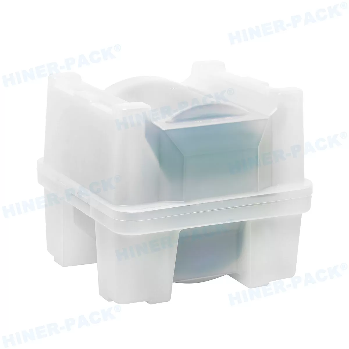
Selection Criteria: What Defines a Leading Wafer Carrier Manufacturer?
Evaluating an industrial wafer packaging supplier requires looking beyond simple box dimensions. Modern transport runs through varied climate zones, air cargo depressurization cycles, and automated handling robotics. We evaluated the world's leading wafer transport suppliers based on four core technical metrics.
- Advanced Polymer Engineering: Safe transit demands engineered resins like conductive polypropylene, ultra-pure polycarbonate, and modified PEEK. The plastic must resist mechanical wear, withstand thermal shifts, prevent particle generation, and maintain strict surface resistivity (typically 105 to 109 ohms/sq) without chemical leaching.
- Tooling Depth and Manufacturing Scale: Injection molding tolerances dictate how securely a wafer rests in its pocket. Top suppliers run clean, precision mold-making workshops. A large portfolio of existing mold assets minimizes upfront NRE (Non-Recurring Engineering) expenses and shortens product delivery times.
- Cleanroom Processing and Washing Lines: Wafer carriers must not add particulate contamination to polished silicon. Manufacturers must operate certified Class 10 to Class 100 cleanrooms equipped with multi-stage ultrasonic deionized water washing systems to ensure zero particle fallout.
- OEM and ODM Agility: Automated fabs use distinct end-effector robotics and handle thinned substrates from 50 to 100 microns. An experienced wafer holders manufacturer must customize slot pitches, cushion rings, and exterior latching systems to fit these non-standard dimensions.
Top 10 Wafer Holders Manufacturers for 2026
1. Hiner-pack (China)
Established in 2013, Hiner-pack has developed into a technical pioneer in semiconductor packaging and precision handling systems. The company specializes in turnkey transport carriers for wafer foundries, compound semiconductor fabs, and OSAT operations worldwide.
Hiner-pack focuses heavily on foundational polymer engineering. Collaborating with advanced domestic material research institutes, the company formulates proprietary ESD-safe, low-outgassing polymers tailored for thin-film and fragile substrates. Their production facility houses high-precision tooling workshops, cleanroom injection lines, and an automated Class 10/100 ultrasonic cleaning line to ensure pristine particle control.
With an active library of over 2,000 production mold sets, Hiner-pack dramatically reduces prototyping schedules and eliminates initial tooling costs for clients. Their product portfolio spans horizontal single-wafer shippers, coin-stack containers, jars, and process cassettes for 2-inch, 4-inch, 6-inch, 8-inch, and 12-inch substrates. Hiner-pack operates as an agile, direct-source manufacturer, offering comprehensive OEM/ODM engineering alongside a growing international distributor network.
2. Entegris (United States)
Entegris remains a prominent global standard-setter in microcontamination control and advanced materials handling. Headquartered in Massachusetts, the company supplies specialized 300mm Front Opening Unified Pods (FOUPs), Front Opening Shipping Boxes (FOSBs), and process cassettes to tier-one foundries.
Their products excel in low-outgassing plastics, automated tracking systems, and automation-friendly mechanical tolerances. While their premium pricing structure can challenge budget-conscious projects, their structural designs remain a benchmark across large automated fabs.
3. Miraial Co., Ltd. (Japan)
Miraial manufactures ultra-clean plastic carriers for semiconductor substrates. The Tokyo-based supplier commands strong market share across East Asia for high-purity PFA horizontal shipping containers and rigid wafer cassettes.
Miraial focuses primarily on extreme material purity. Their shipping systems resist aggressive chemical residues and release virtually no trace metals, making them a top choice for silicon slice manufacturers and bare wafer fabricators.
4. Shin-Etsu Polymer Co., Ltd. (Japan)
As a core subsidiary of the Shin-Etsu Group, Shin-Etsu Polymer leverages internal chemical resources to design high-performance wafer transport boxes. They serve both device makers and bare wafer manufacturers, specializing in 300mm FOSB products and specialized shipping containers.
Their proprietary polymer blends provide consistent static dissipation and strong impact resistance during international air freight. Their integrated supply chain guarantees consistent raw material purity across large product runs.
5. Pozzetta Microhub (United States)
Pozzetta designs secure handling products for semiconductor wafers, reticles, and optical substrates. Located in Utah, the company engineers durable shippers for high-value research lines, compound semiconductor fabs, and military-grade device manufacturers.
Pozzetta designs precision mechanical latches that hold fragile substrates in place without putting stress on delicate edge bevels. Their individual wafer shippers are widely used for low-volume, high-value compound semiconductor transport.
6. 3S Korea Co., Ltd. (South Korea)
3S Korea supplies wafer transport packaging to memory chip producers across South Korea and East Asia. The company focuses on 300mm FOSB units that shuttle bare and processed wafers between wafer manufacturers and memory fabrication lines.
Their FOSB designs feature secure internal clamping and automated latching doors built to match automated stockers. Their products meet standard fab automation metrics and offer a dependable alternative to legacy Japanese suppliers.
7. Gudeng Precision Industrial Co., Ltd. (Taiwan)
Based in Taiwan, Gudeng Precision manufactures front-end mask and wafer carrier equipment. They work closely with top-tier foundry platforms to build EUV mask pods, FOUPs, and specialized thin-wafer shipping cassettes.
Gudeng designs transport frames that shield wafers from ambient humidity and micro-particulates during transport. Their integration with Taiwanese foundries makes them a leading supplier for advanced-node process lines.
8. Dainichi Shoji Co., Ltd. (Japan)
Dainichi Shoji specializes in high-purity process storage, cleanroom cassettes, and transport shippers. The company builds resilient containers for 100mm, 150mm, and 200mm wafers, focusing closely on automotive and legacy-node fabs.
Their designs emphasize mechanical durability and thermal resistance. Fabs that run repeated wet-chemical processing and inter-bay manual transfers rely on their cassettes for long service lifecycles.
9. RTP Company (United States)
RTP Company approaches the carrier market as a custom thermoplastic compounder. While not exclusively a box maker, RTP formulates the structural static-dissipative compounds that many tier-one packaging molders rely on.
Their compounds prevent particulate buildup and control static discharge rates accurately. They help injection molders develop customized structural boxes designed to survive extreme drop, thermal, and friction conditions.
10. Chung Hao Precision Machinery (Taiwan)
Chung Hao manufactures semiconductor shipping cassettes, wafer carriers, and automated handling accessories across Greater China. They specialize in multi-slot cassettes and horizontal storage bins for 6-inch and 8-inch fabrication plants.
Their products offer dependable dimensional stability and seamless integration with mid-generation automated transfer robots. They provide accessible lead times and competitive pricing for secondary foundries and packaging houses.
How Hiner-pack Protects Wafers During Transit
Preventing transport scrap requires engineering solutions that address mechanical shock, electrostatic charges, and surface contamination simultaneously. As a high-precision wafer holders manufacturer, Hiner-pack implements three primary lines of defense across its product catalog.
1. Shock-Absorbing Geometries for Ultra-Thin Substrates
Backgrinding processes commonly thin production wafers down to 75 microns or less. These flexible silicon slices bend and shatter if exposed to resonant road vibration or drop impacts. Hiner-pack designs internal support tracks with micro-cushioning edge tabs that support the inactive exclusion zone of the wafer.
Instead of rigid plastic surfaces, our designs use multi-point elastic contact geometry. These structures absorb drop forces, isolate the substrate from carrier deflection, and keep the active die face completely untouched throughout overseas shipping.
2. Low-Outgassing and Anti-Static Formulations
Standard static inhibitors can migrate to the surface over time, leaving chemical residues on fresh metal layers. Hiner-pack formulates non-migratory carbon-powder networks and inherently dissipative polymers right into the plastic matrix. This prevents static buildup permanently while maintaining electrical surface resistivity between 106 and 109 ohms/sq.
Our raw materials run through thermal vacuum outgassing tests. This guarantees that internal transport environments remain free of harmful siloxanes, plasticizers, and organic outgassing residues that foul thin-film gate oxides.
3. Ultrasonic Class 10/100 Washing Validation
A transport carrier must not add dirt to clean products. Hiner-pack runs all precision shippers through automated multi-stage deionized water ultrasonic wash tanks, followed by filtered HEPA drying inside Class 10/100 environments.
Every product batch undergoes liquid particle count (LPC) and surface ion chromatography testing. Wafers unpack at your customer's dock in the exact pristine state they left your cleanroom.
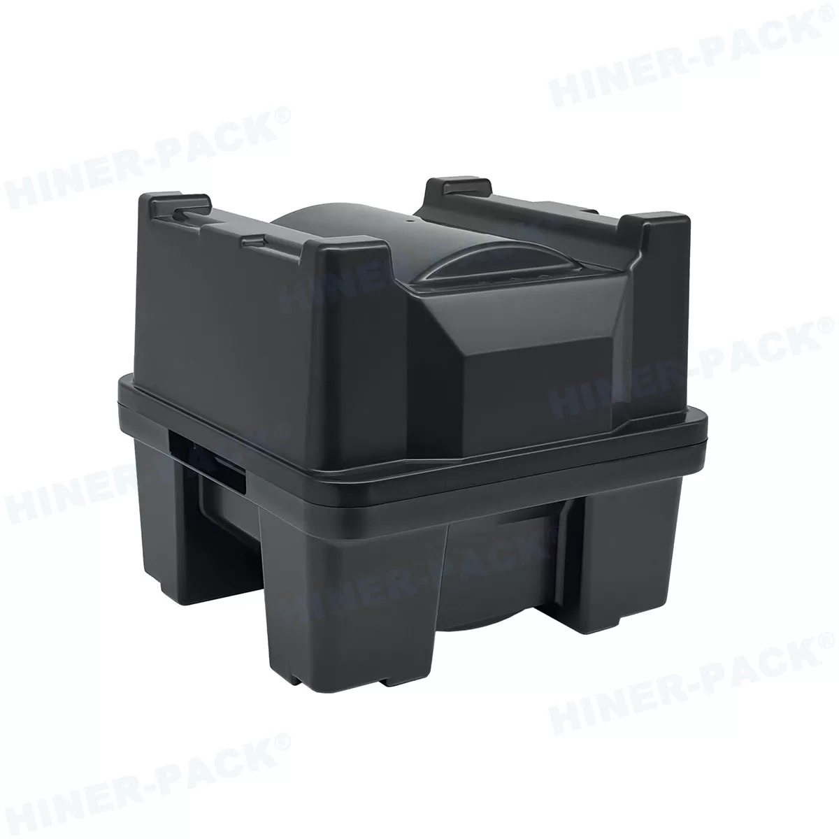
Procurement Checklist: 4 Questions to Ask Your Carrier Supplier
Procuring safe shipping containers requires balancing technical parameters against volume costs. Ask these four core questions before approving a new wafer holders manufacturer.
- 1. Does the carrier material shed particles during standard
vibration profiles?
Demand ASTM D4169 vibration and drop test reports. The internal rails must hold the wafer securely without shedding plastic particles onto the wafer bevel under sustained transit vibration. - 2. Does the supplier cover both small compound substrates and 300mm
silicon?
Compound semiconductors like SiC and GaN use smaller 100mm, 150mm, and 200mm formats, often with non-standard substrate thicknesses. Your supplier should have ready-made tooling for these sizes instead of forcing you into oversized silicon frames. - 3. Are you buying from a direct manufacturer or a trading
agent?
Middlemen mark up prices and slow down technical design iterations. Sourcing directly from an established manufacturing plant like Hiner-pack ensures access to material engineers and eliminates third-party price markups. - 4. What is the real lead time for custom mold
modifications?
Non-standard frame profiles should not require half a year to tool. Ask the vendor how fast they can cut prototype tooling steel and deliver functional evaluation parts to your validation lab.
Frequently Asked Questions (FAQ)
Q1: What materials are standard for semiconductor wafer transport carriers?
A1: Common materials include conductive Polypropylene (PP), Polycarbonate (PC), PBT, and specialty fluoropolymers like PFA. Polycarbonate provides structural rigidity and transparency for single-wafer units. Conductive PP blends offer low-cost, shatter-resistant ESD protection, while high-end PEEK and PFA carriers resist aggressive chemicals during process washing.
Q2: How does a wafer holders manufacturer prevent electrostatic discharge during air shipping?
A2: Manufacturers blend conductive carbon black, carbon nanotubes, or inherently dissipative polymers directly into the raw resin. This creates an interconnected conductive network that safely drains away triboelectric surface charges generated by packaging friction, preventing ESD micro-discharges.
Q3: Can Hiner-pack produce custom-molded wafer holders for non-standard substrate thicknesses?
A3: Yes. Backed by an inventory of over 2,000 existing molds and an in-house tooling workshop, Hiner-pack regularly customizes pocket depths, wafer retention rings, and cassette slot pitches. We engineer specialized solutions for thinned silicon, bonded pairs, optical glass, and brittle compound substrates.
Q4: What is the difference between a wafer cassette and a coin-stack shipper?
A4: A wafer cassette holds substrates vertically in separate individual slots, making it ideal for automated fab tool loading and wet benches. A coin-stack shipper stacks 25 to 50 wafers horizontally, separated by ultra-clean, static-safe interleaf separator pads. Coin-stacks provide high packing density for bulk, cost-efficient transit.
Q5: Why is outgassing critical when evaluating a wafer holders manufacturer?
A5: Low-grade plastics can outgas plasticizers, residual monomers, and volatile organic compounds (VOCs) inside sealed shipping boxes. These airborne airborne molecular contaminants (AMCs) deposit directly onto polished silicon surfaces, contaminating gate oxides and ruining production yields before fabrication even begins.
Secure Your Semiconductor Transport Supply Chain for 2026
Protecting delicate semiconductor substrates during shipment demands proven, particle-free packaging. Shifting wafer sizes, fragile compound materials, and thinner profiles require working with a knowledgeable wafer holders manufacturer that understands polymer science and injection molding.
Hiner-pack combines decades of polymer engineering, thousands of production molds, and high-standard cleanroom washing lines to protect your shipments. We cut production costs, eliminate shipping scrap, and help you hit your yield targets across all global shipping lanes.
Looking for reliable, cost-efficient wafer carriers for your 2026
packaging lines?
Contact the Hiner-pack engineering team today to
review our complete product catalog and receive free product samples for line
qualification.
Grow with our global partner network:
Hiner-pack is
signing authorized distributors worldwide. Partner with us to supply your
regional market with world-class semiconductor packaging solutions directly from
our production lines.














