
As semiconductor manufacturing advances toward 2026 and beyond, front-end fabs and advanced packaging facilities face unprecedented yield challenges. The industry-wide transition toward thinner wafers (<100 μm), wide-bandgap compound semiconductors (SiC and GaN), and high-speed Autonomous Guided Vehicle (AGV) cleanroom logistics has rendered legacy, generic carriers obsolete. In modern automated environments, even sub-millimeter pocket warpage or trace ionic outgassing can trigger automated handler faults and severe yield degradation.
To meet these stringent technical demands, process engineers and procurement teams are bypassing third-party brokers and establishing direct partnerships with specialized manufacturing plants. This technical guide explores the technological standards defining the next generation of semiconductor carriers and explains how partnering with an advanced wafer boat factory like Hiner-pack secures your supply chain for 2026 and beyond.
Upgrading your fab packaging for 2026? Request 2026 qualification samples and 3D CAD step files directly from Hiner-pack.
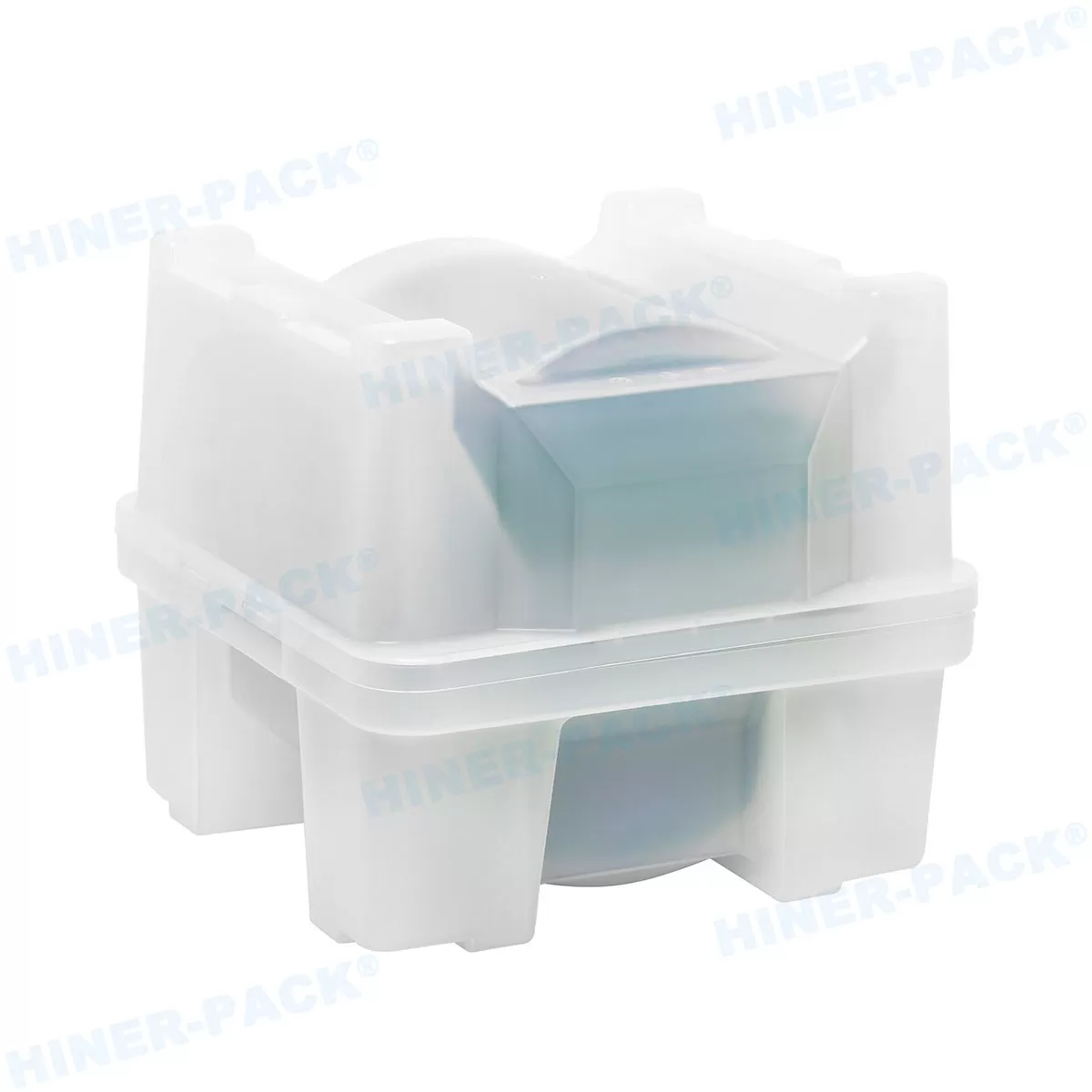
1. Emerging 2026 Fab Requirements Driving Wafer Boat Engineering
The manufacturing specifications for wafer boats, cassettes, and carriers have fundamentally shifted. Modern wafer carrier factories must now design for four critical operational conditions:
High-Speed Robotic Interface: With robotic end-effectors and Equipment Front End Modules (EFEM) operating at higher cycle speeds, wafer slots must maintain dimensional tolerances within ±0.05 mm to eliminate transfer vibration and edge micro-chipping.
Compound Semiconductor Compatibility: Brittle, high-density Silicon Carbide (SiC) and Gallium Nitride (GaN) wafers require customized retention geometries that prevent crystal stress fractures during intra-bay transport.
Permanent, Non-Migrating ESD Control: Advanced node processes cannot tolerate surfactant-based antistatic coatings that leach or decay. Carriers must provide permanent static dissipation ($10^4 - 10^9\ \Omega/\text{sq}$) compliant with ANSI/ESD S20.20 standards.
Strict Outgassing & Trace Metal Limits: High-vacuum and thermal processes require specialized polymer matrices that resist thermal degradation without releasing volatile organic compounds (VOCs) or metallic ions.
2. 2026 Performance Matrix: Advanced Polymers for Wafer Boats
At Hiner-pack, our dedicated Polymer Material R&D Base (developed in partnership with university scientific research institutions) formulates next-generation raw materials engineered for modern fab chemistry and thermal cycling:
| Engineered Polymer Grade | Surface Resistivity (Ω/sq) | Max Thermal Rating | Chemical & Outgassing Profile | Primary 2026 Fab Application |
|---|---|---|---|---|
| Ultra-Clean Conductive PP | 10^4 - 10^6 (Permanent) | Up to 80°C | Low particle generation, standard acid/solvent resistance | Inter-bay AGV transfer, automated sorters, wafer shipping |
| Static-Dissipative Engineered Polymer | 10^6 - 10^9 (Clean ESD) | 80°C - 120°C | Ultra-low ion extraction, DI water compatible | Cleanroom inspection bays, automated pick-and-place lines |
| High-Purity Modified PEEK / PES | 10^6 - 10^9 (or Insulative) | 150°C - 200°C+ | Near-zero VOC outgassing, high steam/solvent resistance | In-line wafer bake ovens, vacuum cure, chemical stripping |
| Fluoropolymer Composites (PFA/PTFE) | Custom Formulations | Up to 260°C | Superior inertness against Hydrofluoric (HF) & harsh acids | Wet bench etching, chemical cleaning, diffusion transfer |
3. Inside Hiner-pack: Advanced Factory Infrastructure & Tooling
Founded in 2013 in Shenzhen, China, Hiner-pack has developed into an integrated high-tech enterprise combining mold design, proprietary polymer development, and high-precision cleanroom injection molding:
Precision Tooling & Mold R&D: In-house high-speed CNC and mirror EDM tooling capabilities allow us to cut and calibrate complex multi-cavity molds with micron-level precision, eliminating draft-angle errors and uneven shrinkage.
Independent Cleanroom Injection Lines: Automated injection molding lines operate in controlled environments, preventing ambient airborne particulate contamination during mold cycling.
Proprietary Material Inventions & Patents: We hold numerous patents in modified conductive polymers, enabling customized color formulations for cleanroom lot management without compromising ESD reliability.
Comprehensive Packaging Portfolio: One-stop factory production covering Wafer Carrier Series (2" to 12"), Shipper Accessories (sponges, cushions), JEDEC Trays, Waffle Packs, and Vacuum Release Gel Boxes.
4. Total Cost of Ownership: Factory-Direct Sourcing vs. Multi-Tier Distribution
Leading fab procurement teams are optimizing their 2026 supply chains by eliminating middleman distributors. Partnering directly with the Hiner-pack factory delivers measurable strategic advantages:
Direct Factory Pricing: Eliminate 15% to 30% markups associated with trading intermediaries and brokers.
Direct Engineering Collaboration: Consult directly with our toolmakers and polymer scientists for customized pocket profiles, custom slot pitches, or DFM optimizations.
Accelerated NRE Tooling Timelines: In-house mold fabrication reduces prototype tooling lead times to 2–3 weeks, accelerating your time-to-market.
Complete Batch Traceability: Every shipment is backed by cleanroom inspection, dimensional CMM data, and certified Certificates of Analysis (COA).
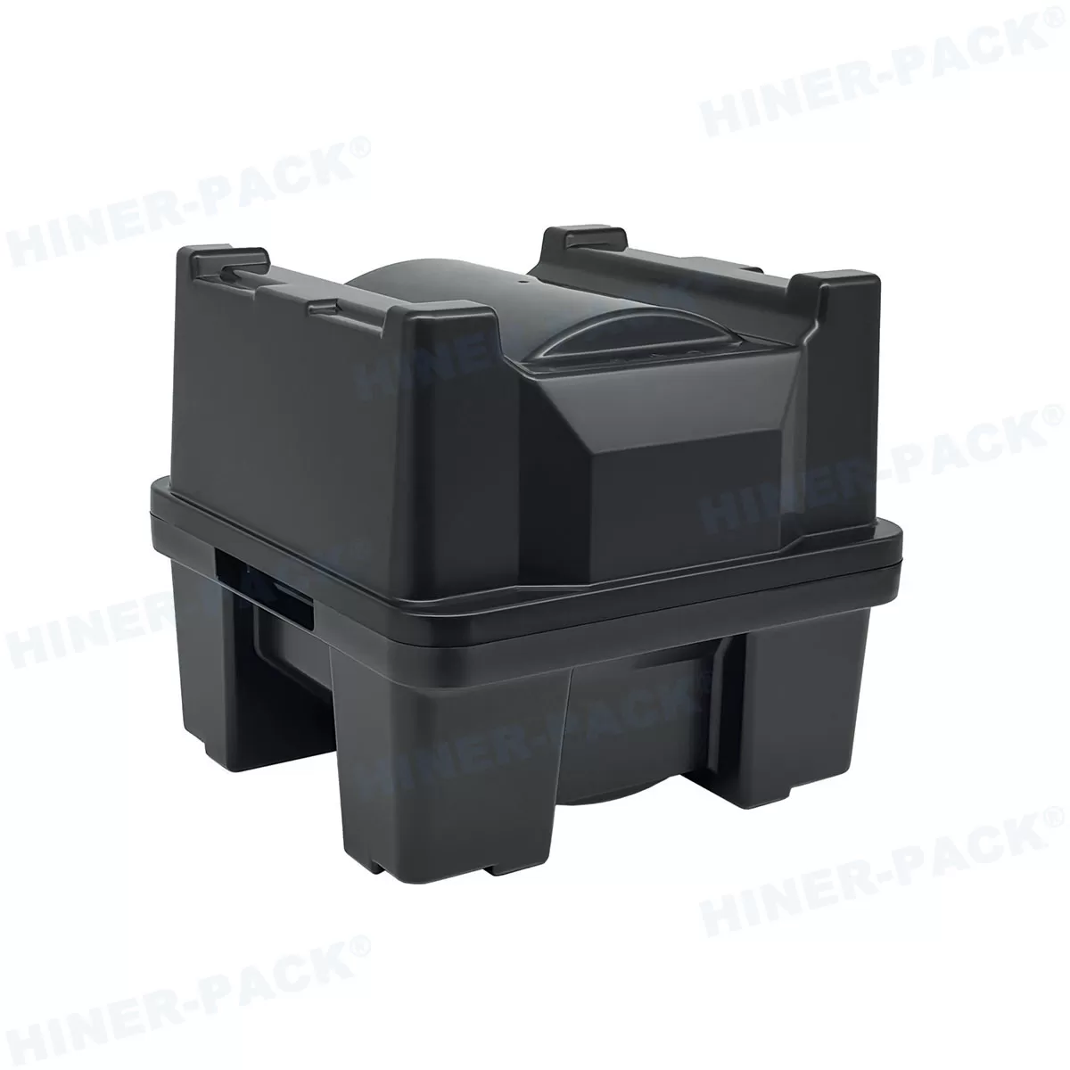
5. 2026 Line-Ready Verification Program
Ensure seamless compatibility with your automated fab equipment and chemical processes before volume release.
What Your Qualification Package Includes:
Free Evaluation Samples: 2 to 5 standard catalog wafer boats or cassettes dispatched within 48 hours for mechanical and automated transfer trials.
Full Technical Data Package: 2D mechanical drawings, 3D .STEP CAD models, and material compliance dossiers (RoHS, REACH, ESD).
Custom Tooling Feasibility Analysis: Free DFM and mold flow analysis for custom substrate dimensions within 24 hours.
Fast-Track Engineering Desk: Contact our technical team at rainbowzhu@hiner-pack.com to initiate your 2026 carrier qualification package.
Frequently Asked Questions About Choosing a Wafer Boat Factory in 2026
Q1: What substrate sizes and carrier configurations can Hiner-pack produce as a direct wafer boat factory?
A1: Hiner-pack manufactures standard and customized wafer boats, cassettes, and storage carriers for 2-inch, 3-inch, 4-inch, 6-inch, 8-inch, and 12-inch wafers. Our portfolio includes 25-capacity multi-wafer cassettes, single-wafer shippers, coin-style carriers, and high-temperature matrix trays designed for silicon, SiC, GaN, and glass substrates.
Q2: How does Hiner-pack address the challenges of handling ultra-thin and compound semiconductor wafers for 2026 fabs?
A2: For ultra-thin wafers (<100 μm) and brittle compound substrates (SiC/GaN), Hiner-pack designs custom cavity profiles with non-contact active areas, beveled edge-retention ribs, and specialized high-elasticity conductive cushioning accessories to prevent crystal micro-cracking and vibration damage during transit.
Q3: How does your factory verify that wafer carriers will not contaminate cleanroom environments?
A3: All carriers are molded from high-purity virgin resins, processed through multi-stage ultrasonic deionized water cleaning systems, and double-vacuum bagged within an ISO-certified cleanroom. Every batch is certified for low particle generation and zero chemical outgassing prior to shipment.
Q4: What is the typical turnaround time for custom wafer boat mold tooling (OEM/ODM)?
A4: Because Hiner-pack operates an in-house mold tooling workshop with dedicated CNC and EDM equipment, custom prototype tooling and First Article Inspection (FAI) samples are completed within 15 to 25 business days following 3D CAD approval.
Ready to future-proof your semiconductor carrier supply chain? Contact our engineering and sales office at rainbowzhu@hiner-pack.com to discuss your requirements with a trusted wafer boat factory














