
In semiconductor wafer fabrication, automated wet chemical processing, and cleanroom transportation, selecting the right carrier is essential to maintaining high device yields. A wafer boat (also known as a wafer cassette or multi-wafer carrier) must provide rigid mechanical stability, sub-millimeter robotic alignment, chemical resistance, and permanent electrostatic discharge (ESD) protection. Substandard carriers can lead to substrate warpage, chemical cross-contamination, or catastrophic wafer edge chipping during automated transfer.
If you are currently evaluating a wafer boat for sale, this comprehensive technical guide provides an overview of available substrate sizes, high-performance polymer formulations, and cleanroom quality benchmarks. Discover how sourcing directly from Hiner-pack provides line-ready semiconductor carriers with factory-direct pricing and rapid sample qualification.
Need immediate pricing and mechanical qualification? Request free evaluation samples and 3D CAD models directly from Hiner-pack.
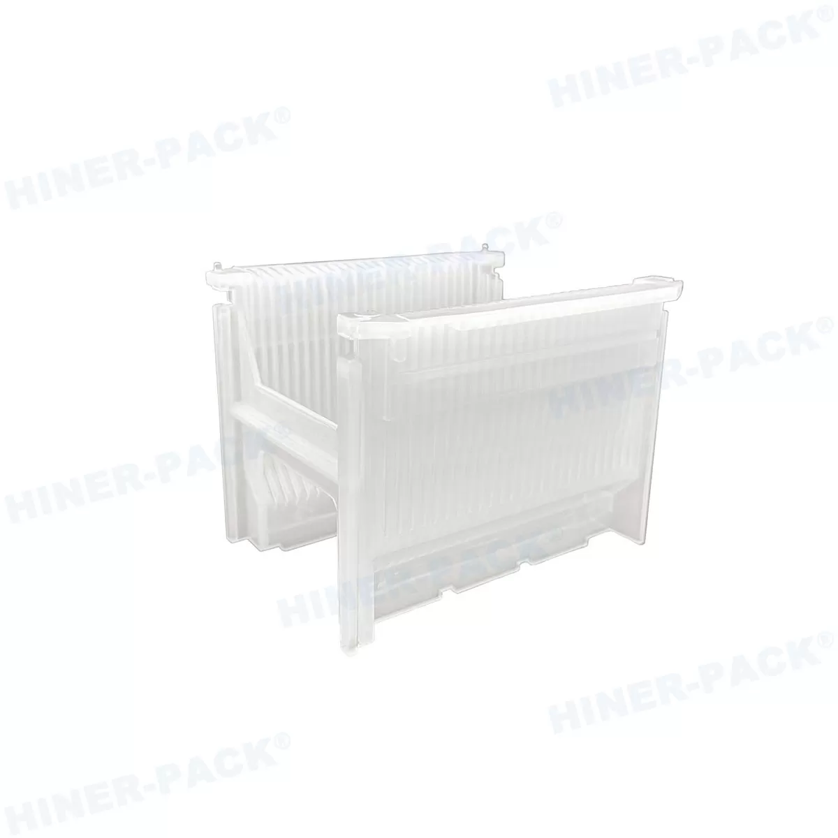
1. Product Catalog: Standard Wafer Boats Available for Sale
At Hiner-pack, we manufacture a comprehensive selection of wafer boats and carriers designed for standard silicon, Silicon Carbide (SiC), Gallium Nitride (GaN), and optical glass substrates:
| Wafer Diameter | Standard Capacity | Available Polymer Formulations | Primary Fab Applications |
|---|---|---|---|
| 2-Inch & 3-Inch | 25 Wafers / Custom | Conductive PP, High-Temp PEEK, Transparent PS | Optoelectronics, compound semiconductors, lab R&D |
| 4-Inch & 6-Inch | 25 Wafers | Conductive PP, Static-Dissipative Resin, PEEK | MEMS fabrication, power device manufacturing, wet bench cleaning |
| 8-Inch (200mm) | 25 Wafers | Conductive PP (SEMI standard), High-Temp PES | Automated front-end fabs, chemical etching, inter-bay AGV transfer |
| 12-Inch (300mm) | 13 / 25 Wafers | Ultra-Clean Conductive PP, Engineered Resins | Advanced node fabrication, automated sorters, FOSB integration |
2. Material Selection: Matching Carriers to Process Chemistry & Temperature
Through our dedicated Polymer Material R&D Base (developed in partnership with university scientific research institutions), Hiner-pack formulates specialized raw materials engineered for diverse semiconductor process conditions:
Conductive Polypropylene (PP): Features permanent surface resistivity ($10^4 - 10^6\ \Omega/\text{sq}$) compliant with ANSI/ESD S20.20 standards. Ideal for ambient shipping, automated sorters, and inter-bay transport up to 80°C.
High-Temperature PEEK / PES: Engineered for thermal stability up to 150°C - 200°C+. Provides near-zero outgassing and high mechanical rigidity during in-carrier baking, vacuum degassing, and aggressive chemical exposure.
Fluoropolymer Blends (PFA / PTFE): Delivers exceptional chemical inertness against Hydrofluoric acid (HF), sulfuric acid, and strong etching solvents during wet bench processing up to 260°C.
Static-Dissipative Modified Polymers: Tailored surface resistance ($10^6 - 10^9\ \Omega/\text{sq}$) with colored raw material options to enable visual lot and fab bay management without shedding conductive particles.
3. Key Quality Benchmarks: What to Check Before You Buy
When reviewing any wafer boat for sale, ensure the supplier verifies the following engineering parameters:
SEMI Dimensional Compliance: Slot pitch, overall pocket depth, and robotic pickup flanges must strictly adhere to SEMI standards to eliminate transfer errors in automated Equipment Front End Modules (EFEM).
Permanent Electrostatic Control: Verify that ESD properties are compounded directly into the polymer matrix rather than applied as temporary surfactant coatings that wash away in DI water.
Zero Particle Shedding: Cavities must feature mirror-polished surfaces to minimize mechanical abrasion and edge-bead particulate generation during loading.
Cleanroom Processing: Finished carriers should undergo multi-stage ultrasonic deionized water cleaning and double-vacuum bagging in an ISO-certified cleanroom.
4. Why Buy Factory-Direct from Hiner-pack?
Founded in 2013 in Shenzhen, China, Hiner-pack is an integrated high-tech enterprise. Purchasing directly from our manufacturing plant delivers measurable procurement advantages:
Direct Factory Pricing: Eliminates middleman markups from distributors and trading companies, lowering unit costs by 15% to 30%.
In-House Precision Tooling: High-speed CNC and EDM mold workshops enable rapid customization for non-standard substrate thicknesses and shapes.
Comprehensive Packaging Portfolio: One-stop sourcing for Wafer Carrier Series, Wafer Shipper Accessories (conductive sponges, cushions), JEDEC Trays, Waffle Packs, and Vacuum Release Gel Boxes.
Strict Quality Traceability: Every production batch is inspected with optical CMM laser systems and surface resistivity testers to guarantee dimensional and electrical compliance.
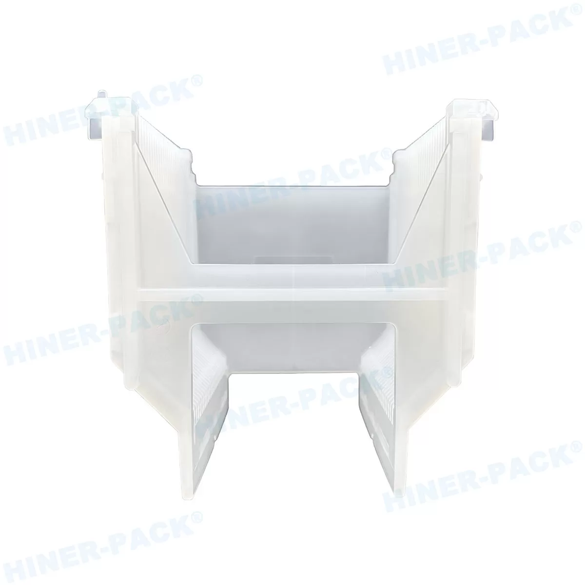
5. 3-Step Free Sample & Fast-Track Purchasing Program
Qualify our wafer boats on your automated equipment before placing commercial orders.
How the Process Works:
Submit Your Requirements: Specify your required wafer diameter, process temperature, chemical exposure, and estimated annual batch volume.
Receive Fast Engineering Feedback: Our technical team provides a formal quotation, 3D .STEP CAD files, and material compliance certificates within 24 hours.
Sample Testing & Verification: Standard catalog evaluation samples are dispatched within 48 hours for immediate mechanical fit and ESD testing.
Direct Purchasing Desk: Send your RFQ directly to rainbowzhu@hiner-pack.com for immediate factory support.
Frequently Asked Questions About Wafer Boat for Sale
Q1: What sizes and types of wafer boat for sale does Hiner-pack keep in stock?
A1: Hiner-pack maintains inventory of standard 2", 3", 4", 6", 8", and 12" multi-wafer cassettes (25-wafer capacity), single-wafer shippers, and coin-style boxes in conductive PP and static-dissipative polymers. Standard catalog items ship within 24 to 48 hours of order confirmation.
Q2: Can I purchase custom-engineered wafer boats for non-standard substrate thicknesses or fragile materials?
A2: Yes. For ultra-thin silicon (<100 μm), Silicon Carbide (SiC), Gallium Nitride (GaN), or custom optical glass, our in-house mold R&D center designs custom cavity pockets and non-contact bevel retention ribs. Prototype tooling and First Article Inspection (FAI) samples are completed in 15 to 25 business days.
Q3: How does Hiner-pack ensure that wafer boats for sale meet cleanroom particle standards?
A3: All carriers are injection-molded using virgin polymers in controlled environments, processed through multi-stage ultrasonic deionized water washing stations, and double-vacuum bagged in an ISO cleanroom to ensure zero particle shedding upon delivery.
Q4: What is the minimum order quantity (MOQ) when purchasing wafer boats from Hiner-pack?
A4: For standard catalog inventory, we support flexible trial quantities starting from 10 to 50 units for engineering line qualification. For customized OEM/ODM projects requiring dedicated mold fabrication, volume pricing and batch MOQs are determined based on tooling cavitation and resin compounding specs.
Ready to purchase line-ready semiconductor carriers? Contact our technical sales engineering team at rainbowzhu@hiner-pack.com to request your factory-direct quote on any wafer boat for sale today.














