
In automated wafer fabrication, wet chemical processing, and cleanroom transportation, wafer boats (also referred to as wafer cassettes and multi-wafer carriers) are critical handling components. A defect in dimensional tolerance, minor polymer outgassing, or inadequate electrostatic dissipation can result in robotic transfer errors, chemical cross-contamination, or severe wafer cracking.
Selecting the right wafer boat manufacturer requires an in-depth evaluation of material compounding capabilities, mold precision, cleanroom manufacturing standards, and SEMI specification compliance. This engineering guide breaks down the essential technical criteria for sourcing high-reliability wafer boats and highlights how partnering directly with Hiner-pack safeguards your fab's automated throughput and device yields.
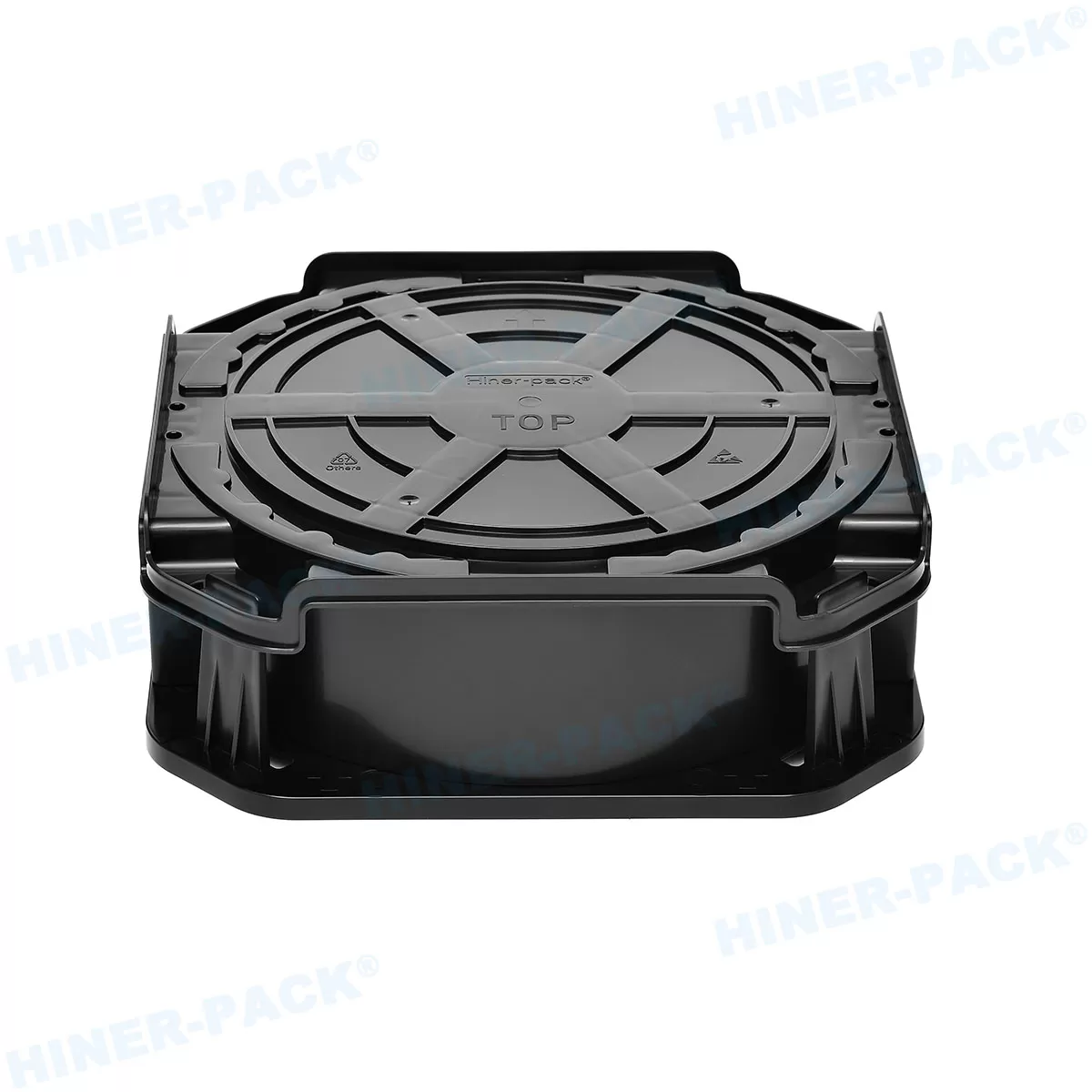
Need to qualify wafer boats for your fab line? Request evaluation samples and 3D CAD models directly from Hiner-pack.
1. Key Engineering Criteria When Evaluating a Wafer Boat Manufacturer
A reliable wafer carrier manufacturer must engineer products that perform reliably under mechanical stress, thermal cycling, and aggressive chemical exposure. When vetting suppliers, focus on four core manufacturing capabilities:
Precision Slot Pitch & Geometric Stability: Automated robotic end-effectors require exact slot spacing and minimal sidewall deflection. Sub-millimeter tolerances prevent wafer misalignment during rapid pick-and-place cycles.
Permanent Electrostatic Discharge (ESD) Control: Static charges attract airborne particulates and cause ESD events. Carriers must feature permanently integrated static-dissipative ($10^6 - 10^9\ \Omega/\text{sq}$) or conductive ($10^4 - 10^6\ \Omega/\text{sq}$) matrix networks that do not wash off during chemical processing.
Chemical Inertness & Low Trace Metals: Carriers used in wet bench cleaning or etching must withstand harsh acids, solvents, and deionized water without leaching metallic ions or volatile organic compounds (VOCs).
High-Temperature Dimensional Integrity: For bake-out, drying, or high-temperature storage, materials must resist continuous thermal exposure without warping or pocket deformation.
2. Material Selection Matrix for Semiconductor Wafer Boats
At Hiner-pack, our dedicated Polymer Material R&D Base (established in collaboration with university research institutes) develops proprietary polymer formulations tailored to specific fab process requirements:
| Polymer Formulation | Surface Resistivity (Ω/sq) | Continuous Thermal Rating | Chemical Resistance | Primary Fab Applications |
|---|---|---|---|---|
| Conductive Polypropylene (PP) | 10^4 - 10^6 (Conductive) | Up to 80°C | Moderate (General solvents/acids) | Inter-bay transport, shipping, automated sorting systems |
| Static Dissipative Engineered Resins | 10^6 - 10^9 (ESD-Safe) | 80°C - 120°C | High (DI water, light acids) | Cleanroom automated handling, inspection lines |
| High-Temp Modified PEEK / PES | 10^6 - 10^9 (or Insulative) | 150°C - 200°C+ | Excellent (High chemical & steam resistance) | In-line baking, vacuum cure ovens, harsh chemical baths |
| Fluoropolymer Blends (PFA / PTFE) | Custom Formulations | Up to 260°C | Superior (HF, aggressive etching acids) | Wet bench etching, chemical cleaning, diffusion transfer |
3. Robotic Compatibility & Precision Mold Tooling
Automated front-opening shipping boxes (FOSBs), automated guided vehicles (AGVs), and robotic end-effectors require complete adherence to SEMI dimensional standards. Sourcing from a manufacturer with in-house tooling capabilities is essential:
CNC & EDM In-House Tooling: Eliminates third-party mold inaccuracies, ensuring precise pocket contours, robotic pickup notches, and flat/notch alignment.
Anti-Abrasion Cavity Finishing: Mirror-polished mold cavities reduce friction along wafer bevels, minimizing edge chipping and microscopic particle generation.
Warpage Control Technology: Advanced multi-point injection gating ensures balanced shrinkage during cooling, preserving dimensional stability across temperature variations.
4. Direct Manufacturer Strengths: Why Partner with Hiner-pack?
Founded in 2013 in Shenzhen, China, Hiner-pack has grown into an integrated high-tech enterprise with independent injection molding lines, proprietary polymer research, and a comprehensive portfolio of semiconductor carrier solutions:
One-Stop Turnkey Sourcing: Beyond wafer boats and cassettes (2", 3", 4", 6", 8", and 12"), we manufacture Wafer Shipper Accessories (conductive cushions, gaskets), JEDEC IC Trays, Bare Die Waffle Packs, and Vacuum Release Gel Boxes.
Proprietary Material Patents: Our engineering team holds numerous patents in modified antistatic formulations, enabling custom colored materials for visual lot tracking in cleanrooms.
Full Process Quality Control: Equipped with optical coordinate measuring machines (CMM), surface resistance testers, and cleanroom particulate monitoring systems to certify every production batch.
Bespoke OEM/ODM Customization: Rapid DFM analysis and fast tooling development for specialized substrate materials, including Silicon Carbide (SiC), Gallium Nitride (GaN), and ultra-thin substrates.
3-Step Engineering Verification & Sample Testing Program
Ensure total process compatibility before approving volume procurement orders.
What Your Qualification Package Includes:
Functional Test Samples: Evaluation wafer boats/cassettes dispatched for robotic handler and chemical bath testing.
Complete Technical Documentation: 2D mechanical drawings, 3D .STEP CAD files, and Certificates of Analysis (COA) for ESD and material purity.
Direct Factory Pricing: Tiered volume quotations direct from our manufacturing facility, free of broker markups.
How to Request Your Carrier Kit:
Submit Your Specifications: Send your wafer diameter, chemical/thermal exposure levels, and process requirements to our technical sales team.
DFM & Tooling Review: Our tooling engineers verify drawing compatibility and confirm material specifications within 24 hours.
Sample Delivery: Cleanroom-packed qualification samples are dispatched via express courier within 48 hours.
Fast-Track Engineering Desk: Contact our team at rainbowzhu@hiner-pack.com for fast technical assistance.
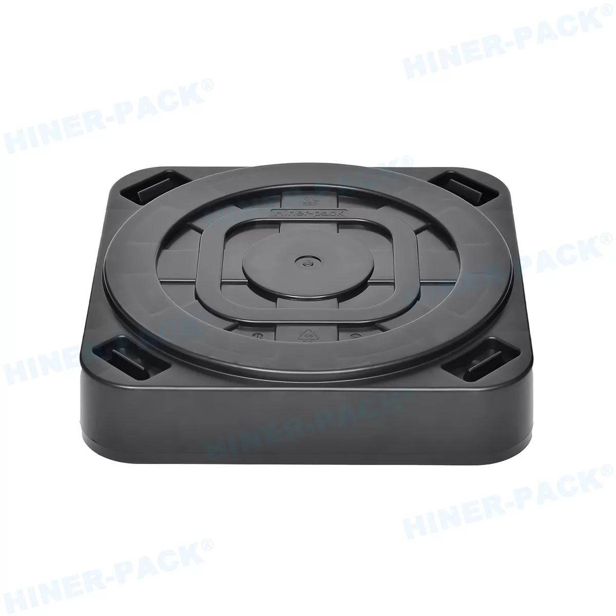
Frequently Asked Questions About Choosing a Wafer Boat Manufacturer
Q1: What substrate sizes and carrier types can Hiner-pack manufacture as a wafer boat manufacturer?
A1: Hiner-pack manufactures standard and customized wafer boats, cassettes, and carriers for 2-inch, 3-inch, 4-inch, 6-inch, 8-inch, and 12-inch wafers. Our portfolio spans 25-capacity multi-wafer cassettes, single-wafer shippers, coin-style carriers, and high-temperature matrix trays designed for silicon, SiC, GaN, and glass substrates.
Q2: How does Hiner-pack guarantee chemical and thermal resistance in its wafer carriers?
A2: Through our dedicated polymer R&D lab and university research partnerships, we formulate specialty high-performance resins—including modified PEEK, PES, and fluoropolymer compounds. Every material batch undergoes rigorous testing for continuous thermal resistance (up to 200°C+) and chemical inertness against common acids and solvents.
Q3: Can Hiner-pack develop custom wafer boats for non-standard automated equipment?
A3: Yes. As an integrated OEM/ODM manufacturer with in-house CNC and EDM tooling facilities, we develop custom pocket profiles, modified robotic flange interfaces, and tailored slot pitches. Our engineering team provides full DFM analysis and 3D CAD models within 1 to 2 business days.
Q4: Why should semiconductor fabs source directly from Hiner-pack rather than third-party distributors?
A4: Sourcing directly from Hiner-pack eliminates third-party markups (saving 15%–30% in procurement costs), shortens tooling and sample lead times, and provides direct engineering access for material modifications and strict cleanroom-controlled batch traceability.
Ready to elevate your wafer handling reliability? Contact our engineering desk at rainbowzhu@hiner-pack.com to discuss your requirements with a trusted wafer boat manufacturer today.














