
The global semiconductor industry is moving rapidly toward sub-3nm nodes and complex 3D packaging designs. In this high-stakes environment, even microscopic contamination can ruin an entire production batch. Yield loss during wafer transport and storage is an expensive bottleneck that packaging facilities must prevent.
Securing a reliable wafer container supplier is no longer just a routine procurement task. It is a critical risk-management strategy that directly affects your bottom line. This article provides a structured framework to evaluate suppliers based on material science, contamination control, and supply chain reliability.
The Core Challenge: Why Wafer Protection is Becoming Harder
Wafers are becoming thinner, larger, and far more fragile. During transit between fabrication facilities and packaging plants, wafers face mechanical shocks, electrostatic discharge (ESD), and outgassing. Traditional storage solutions are often insufficient for modern high-density interconnects.
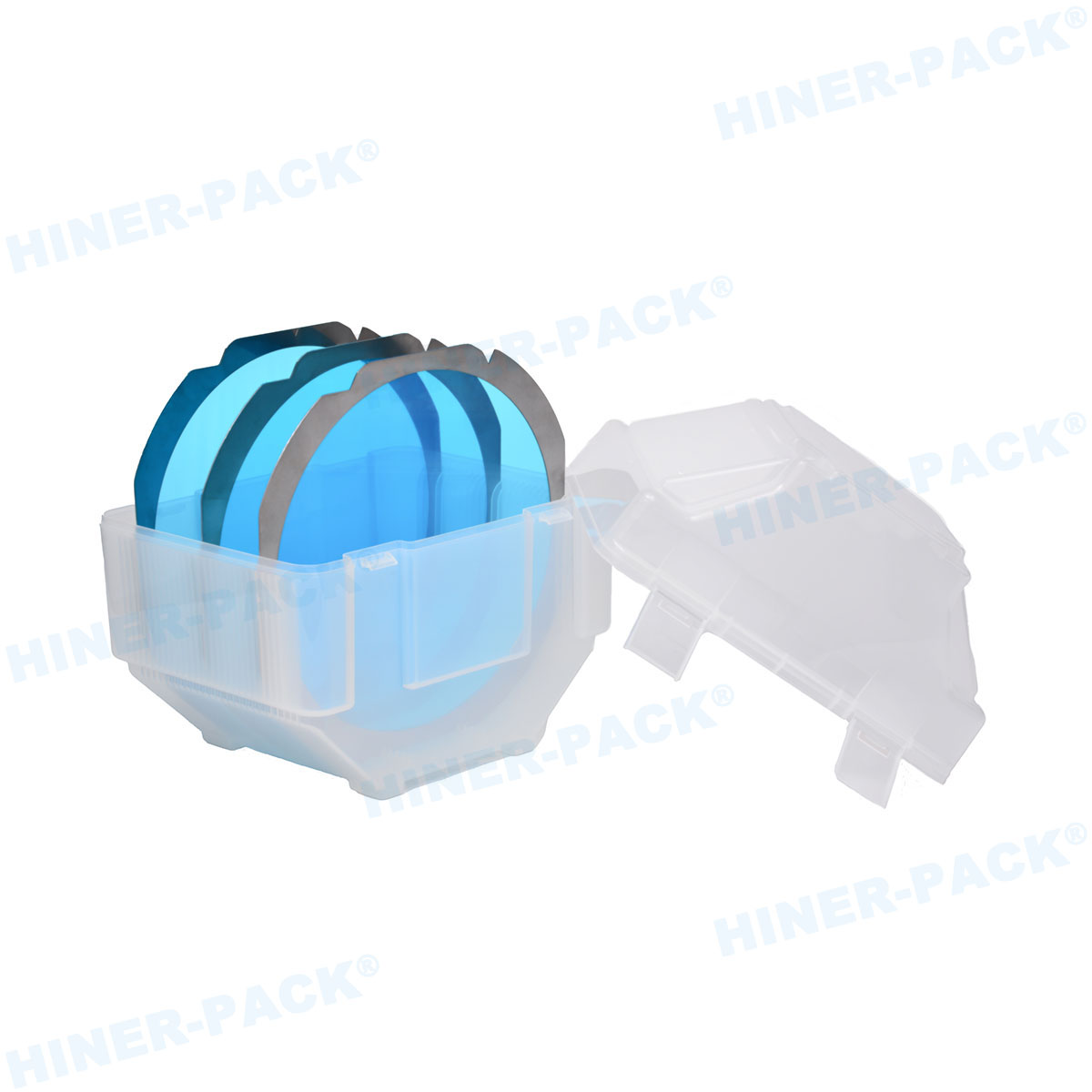
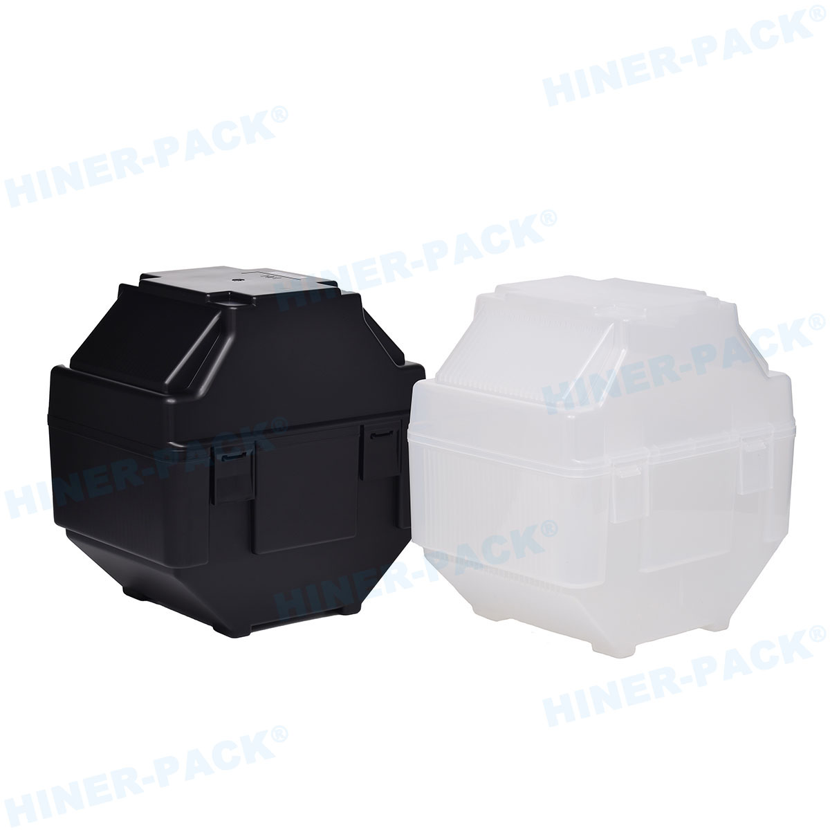
Physical contamination from airborne particles or outgassing can corrupt delicate wafer patterns. To prevent this, leading packaging engineers partner with specialized manufacturers like Hiner-pack. These manufacturers design specialized wafer carriers that protect sensitive materials from environmental hazards.
When selecting a wafer container supplier, engineering teams must look beyond unit costs. A low-cost carrier that fails to manage static charge or sheds micro-particles can cause millions of dollars in yield loss.
The "3-S Shield" Framework for Wafer Container Evaluation
To help procurement and quality engineering teams make informed decisions, we developed the "3-S Shield" Framework. This systematic approach focuses on three core pillars: Structural Integrity, Surface Chemistry, and Static Control.
Evaluating a prospective wafer container supplier against these three pillars helps ensure your wafer carriers can withstand real-world transport risks.
1. Structural Integrity (Mechanical Protection)
Wafer containers must absorb mechanical vibrations and impacts during transit. Look for suppliers who use high-impact polymers and precise molding tolerances. This prevents the wafer from moving inside the carrier, which can cause micro-cracks and edge chipping.
2. Surface Chemistry (Contamination Control)
The container materials must not release volatile organic compounds (VOCs). Outgassing can deposit thin chemical films on the wafer surface, interfering with lithography or wire bonding. A reliable wafer container supplier should provide comprehensive outgassing test reports, such as GC-MS analysis.
3. Static Control (ESD Protection)
Electrostatic discharge can destroy thin-gate oxides on integrated circuits. Wafer carriers must use specialized carbon-filled or inherently dissipative polymers. These materials safely bleed off static charges without shedding carbon particles that could contaminate the cleanroom.
The Counter-Intuitive Truth: The "Over-Specification" Trap
A common mistake among packaging engineers is assuming that the most expensive, ultra-high-purity (UHP) material is always the best choice. This "over-specification" can actually introduce unexpected engineering risks and inflate production budgets.
For example, some high-purity polymers designed for wet-bench processing are highly insulative. If used for shipping containers, they can build up static charge during transport. This static charge attracts airborne dust, increasing the risk of physical contamination.
Rather than simply requesting the highest grade of plastic, work with a collaborative wafer container supplier to find the right balance. Highly engineered polymers, such as those offered by Hiner-pack, provide balanced ESD protection and low outgassing properties without unnecessary material costs.
Operational Checklist: Auditing Your Wafer Container Supplier
Use this technical checklist during your next supplier audit or Request for Proposal (RFP) process. It ensures the manufacturer meets the rigorous standards required for semiconductor packaging.
| Evaluation Metric | Industry Standard / Target | Why It Matters |
|---|---|---|
| Surface Resistivity | 105 to 1011 ohms/sq (Static Dissipative) | Prevents ESD damage while minimizing particle attraction. |
| Cleanroom Packaging | ISO Class 4 or Class 5 environment | Ensures containers do not bring contaminants into your cleanroom. |
| Outgassing Limits | Low VOC emissions (ASTM E595 testing) | Prevents molecular contamination on active wafer surfaces. |
| Traceability | Batch-level resin tracking | Allows rapid root-cause analysis if a material defect occurs. |
| Dimensional Tolerance | ASME Y14.5 compliant molding | Ensures seamless compatibility with automated tracking systems. |
Anticipated Doubts: Frequently Asked Questions
Q1: How do I verify the cleanroom compatibility of a wafer shipping box?
A1: A reputable wafer container supplier should provide Liquid Particle Count (LPC) and Ion Chromatography (IC) reports. These tests measure the extractable ionic contamination and particulate levels on the container surface, confirming they meet cleanroom standards.
Q2: Why is polycarbonate (PC) commonly used for wafer shippers instead of polypropylene (PP)?
A2: Polycarbonate offers superior dimensional stability, impact resistance, and transparency. This allows operators to inspect wafers visually without opening the container. Polypropylene is softer and more prone to deformation under mechanical stress.
Q3: How does Hiner-pack ensure batch-to-batch consistency in ESD properties?
A3: Hiner-pack utilizes precise, automated compounding processes. They measure the surface resistivity of every production lot to ensure the conductive additives are evenly distributed throughout the polymer matrix.
Q4: Can wafer containers be safely reused across multiple shipping cycles?
A4: Some containers can be reused, but they must undergo validated cleaning cycles. Over time, plastic can degrade, lose its ESD properties, or accumulate stubborn residues. For critical, high-value wafers, single-use shipping is often recommended to minimize contamination risks.
Q5: What lead times should I expect from a reliable wafer container supplier?
A5: Standard lead times typically range from 2 to 6 weeks, depending on the customization required. It is best to choose a wafer container supplier that maintains safety stock of common sizes, helping you avoid production delays during sudden market swings.
Choosing a Collaborative Partner
As semiconductor packaging technologies continue to advance, the demands placed on wafer transport logistics will only grow. Protecting your yield requires more than just buying plastic boxes. It demands a deep understanding of polymer science, cleanroom logistics, and contamination control.
When selecting your next wafer container supplier, focus on technical transparency and collaborative engineering. Partners like Hiner-pack offer the materials, cleanroom manufacturing, and quality control systems needed to protect your wafers.
If you want to optimize your wafer packaging workflow and protect your yields, contact our engineering team today to request material samples and discuss your specific application needs.


