
The shift toward 300mm substrates, ultra-thin dies, and heterogeneous integration places unprecedented demands on wafer handling and storage. A single defect caused by particle shedding, electrostatic discharge (ESD), or chemical outgassing can destroy high-value devices. This is why semiconductor fabs, OSATs (outsourced semiconductor assembly and test), and foundries evaluate a wafer container manufacturer based on more than price—it involves material purity, mechanical shock isolation, and long-term dimensional stability. In this deep-dive, we examine engineering parameters, cleanroom protocols, and validation methods that separate qualified suppliers from the rest. Companies like Hiner-pack apply decades of injection molding and contamination control expertise to address these industry challenges.
1. Core Functions of a Wafer Container Manufacturer in Modern Semiconductor Flows
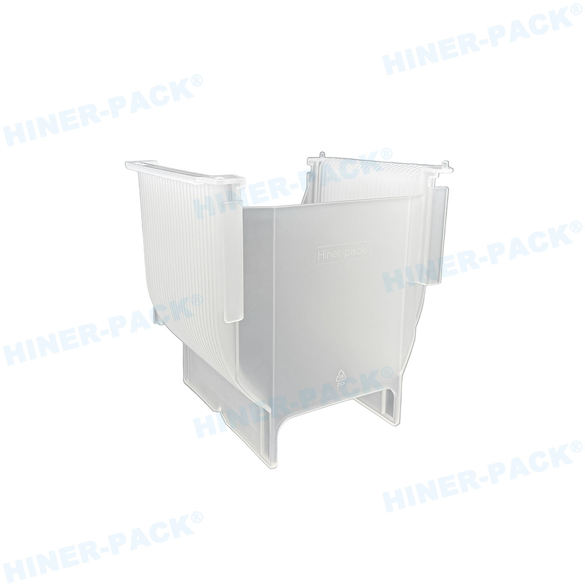
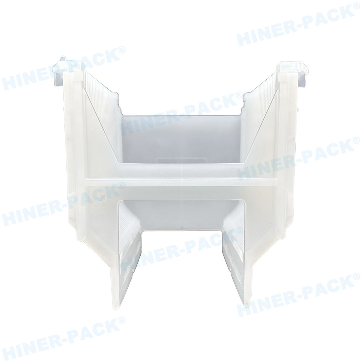
Wafer containers—including front opening unified pods (FOUPs), front opening shipping boxes (FOSBs), and wafer shippers—protect substrates from fab to packaging. Their roles extend beyond simple physical protection. A professional wafer container manufacturer ensures:
Particle control: Internal surfaces must maintain ≤0.1μm particle adders per 300mm wafer exposure.
Moisture and oxygen barrier: For sensitive copper-low-k or MEMS devices, low water-vapor transmission rates (WVTR) are mandatory.
ESD-safe properties: Surface resistivity between 10⁵–10¹¹ Ω/sq prevents charge accumulation.
Automation compatibility: Precise kinematic coupling, mapping slots, and RFID integration for tool communication.
Failures in any function propagate yield loss. For instance, high-friction container ribs might scratch wafer backside, generating particles that later cause lithography defects. Therefore, advanced manufacturers design containers using computational fluid dynamics (CFD) to minimize turbulent airflow during door opening.
2. Material Science & Cleanroom Compliance – Core Competencies
Polycarbonate (PC) and polyetheretherketone (PEEK) blends dominate wafer container construction. However, base resin purity is only the starting point. A specialized wafer container manufacturer focuses on:
2.1 Low-Outgassing Formulations
Outgassing species (e.g., cyclosiloxanes, amides, plasticizers) condense onto wafer surfaces, altering photoresist adhesion or gate oxide properties. Manufacturers employ gas chromatography-mass spectrometry (GC-MS) to verify outgassing below SEMI S2/S8 limits. Hiner-pack uses 100% virgin, semiconductor-grade polymers without mold-release additives.
2.2 Static Dissipative Technologies
ESD events create latent defects like gate oxide rupture. Container manufacturers integrate carbon nanotubes or inherently dissipative polymers (IDPs) to achieve stable static decay <0.5 seconds. Regular audits check surface resistivity after repeated cleanings, as surfactants can leach anti-static agents.
2.3 Cleanroom Assembly & Packaging
Containers assembled in ISO Class 4 (Fed Std 209E Class 10) environments, then double-bagged in nitrogen-purged film, reduce airborne molecular contamination (AMC). Each batch receives particle count validation using liquid particle counters (LPCs) from critical surfaces.
3. Engineering Challenges for 300mm, Warped, and Thin Wafers
Wafer warpage after backgrinding (up to ±5mm for thin dies) challenges conventional container designs. Standard FOUP slots with rigid supports cause edge cracking or die shifting. Advanced solutions include:
Adjustable pitch and curved slot profiles: Custom designs from a responsive wafer container manufacturer accommodate warped wafers without stress concentration.
Soft-contact retention mechanisms: Flexible side grippers replace rigid posts, distributing clamping force evenly.
Vacuum-release features: Prevent wafer-drag when opening container lids in cleanroom vacuums.
For wafer-level packaging (WLP) where dies are directly processed on the substrate, container internal humidity control becomes critical. Some manufacturers embed desiccant channels or vapor-phase corrosion inhibitors (VpCI) into lid designs. Additionally, RFID-enabled containers track time-sensitive process steps, notifying operators when wafers exceed floor life.
4. Advanced Manufacturing Processes for High-Performance Wafer Containers
Producing sub-0.5mm dimensional accuracy across large FOUP bodies (over 700mm length) requires specialized injection molding presses with real-time cavity pressure monitoring. Below are processes elite suppliers utilize:
4.1 Multi-Stage Injection with Gas-Assist
Prevents sink marks and internal stress that later warps during autoclave cleaning. Molds designed with conformal cooling channels reduce cycle time while maintaining flatness below 0.2mm per meter.
4.2 Automated Deburring & Laser Marking
Residual flash from parting lines generates particles. High-volume manufacturers use robotic trimming and CO₂ laser ablation to remove micro-burrs. Laser marking also applies 2D Data Matrix codes for traceability per SEMI T7.
4.3 Ultrasonic Welding for Double-Wall Insulation
For temperature-sensitive wafers (e.g., InP or GaAs), double-wall containers offer thermal buffering. Ultrasonic welding ensures particle-free joints without adhesives that outgas. Each weld strength is verified via peel tests.
Additionally, a top-tier wafer container manufacturer provides certificate of conformance (CoC) reports that include dimensional reports, particle mapping, and ESD decay data per shipment batch. Hiner-pack's production line integrates in-line vision systems to inspect slot coplanarity and latch functionality.
5. Selecting a Qualified Wafer Container Manufacturer: Key Evaluation Metrics
When sourcing containers for high-volume manufacturing (HVM) or R&D pilot lines, buyers should request objective evidence for the following parameters:
Particle performance: SEMI E154 (FOUP) or E150 (FOSB) testing, showing <10 particles >0.1μm added per wafer after 1000 robot insertions.
Chemical compatibility: Resistance to standard fab cleaning agents (IPA, H₂O₂, NH₄OH) without surface degradation.
Mechanical durability: 50,000+ open/close cycles on latch mechanisms without particle generation.
Certifications: ISO 14644-1 Class 1-3 assembly environment, plus IATF 16949 for process control.
Custom engineering support: Ability to modify slot pitch, add foam inserts for thin-glass wafers, or redesign mapping slots.
Reputable suppliers willingly provide test wafers for on-site qualification runs. Additionally, they offer 3D CAD models for automation integration studies. Note that a manufacturer's experience with high-aspect-ratio containers (e.g., 25-slot FOUPs for 300mm) directly reduces your tool downtime due to handling errors.
6. Future Trends: Embedded Sensors and Enhanced Traceability
Industry 4.0 adoption is influencing wafer container design. Upcoming requirements include:
Embedded humidity and vibration sensors that log transportation shocks; data retrieved via near-field communication (NFC).
Color-changing indicators for oxygen or moisture exposure, particularly for wafers with reactive metal layers.
Digital twin integration – container identification linked to automated material handling system (AMHS) to predict cleaning schedules.
Forward-looking wafer container manufacturer partners are already prototyping connectors for in-container microenvironments. Hiner-pack, for example, offers RFID-ready FOSBs and consults on sensor placement without compromising seal integrity.
Frequently Asked Questions (FAQ) about Wafer Container Manufacturing
Q1: What cleanliness level should I expect from a wafer container
manufacturer?
A1: Container internal surfaces must meet ISO Class 3
(FS209E Class 1) particle counts after cleaning. Reputable suppliers ship
containers double-sealed with certificates showing liquid particle counter
results for each batch. Look for <10 particles >0.3μm per 100cm².
Q2: How do I validate a new FOUP design for my specific wafer
warpage?
A2: Request a finite element analysis (FEA) report from the
manufacturer showing contact pressure distribution. Additionally, run a pilot
batch with dummy wafers coated with dye-check developer; inspect for contact
marks. A competent wafer container
manufacturer provides 3D-printed prototypes for fit-check before
steel mold fabrication.
Q3: Can wafer containers be recycled or reground after
end-of-life?
A3: Yes, but regrinding must be carefully controlled to
avoid contamination. Some manufacturers, including Hiner-pack, operate take-back
programs where used containers are shredded, purified, and repurposed into
non-critical products. However, for critical FOUPs, virgin material is always
recommended.
Q4: What is the typical lead time for custom injection-molded wafer
containers?
A4: Developing a new mold takes 12–16 weeks, followed by
2–3 weeks for qualification runs. A manufacturer with in-house tooling (like
Hiner-pack) reduces coordination delays. For semi-custom designs (modified slot
configurations), lead times drop to 4–6 weeks.
Q5: How often should wafer containers be requalified?
A5:
SEMI guidelines recommend requalification every 12 months or after 500 cleaning
cycles, whichever comes first. Monitoring parameters include particle
generation, ESD resistivity, and latch torque. The manufacturer should provide
requalification protocols.
Q6: Do I need different containers for wafer shipping vs. in-fab
storage?
A6: Yes. Shipping containers (FOSBs) prioritize mechanical
shock absorption and double-wall insulation, while in-fab FOUPs focus on
automation interface and low outgassing. A full-service wafer
container manufacturer offers both categories with compatible
kinematic bases.
Conclusion & Inquiry for Your Specific Wafer Handling Needs
Selecting a wafer container manufacturer directly impacts die yield, equipment uptime, and cross-fab logistics. The industry's movement toward larger panels, ultra-thin substrates, and faster cycle times demands more than off-the-shelf solutions. Prioritize suppliers that demonstrate in-house material modification, cleanroom molding, and transparent test data. For OSATs and IDMs evaluating next-generation container designs, reaching out to a specialist like Hiner-pack allows you to benchmark current containers against application-specific requirements.
Ready to discuss your wafer handling challenges?
→ Submit
your wafer size (150/200/300mm), warpage range, and cleanroom class to receive a
tailored proposal. Our engineering team provides sample qualification and
contamination analysis.
Send inquiry now: https://www.waferboxes.com/contact.html (or use the contact form on our website). All inquiries receive a detailed
technical datasheet and dimensional report within 48 hours.


