
The semiconductor manufacturing supply chain requires extreme precision at every step, extending beyond the cleanroom of the foundry to the logistics and packaging materials that protect silicon wafers during transit. As node sizes shrink to single-digit nanometers, the vulnerability of microelectronic structures to physical, chemical, and electrostatic damage increases significantly. Even minor particulate contamination or a brief electrostatic discharge event can lead to severe yield loss across an entire production lot. Consequently, selecting a specialized wafer box factory is an important decision for procurement and quality assurance teams at foundries and outsourced semiconductor assembly and test (OSAT) facilities.
A high-performance wafer transport container, such as a coin box, wafer jar, or multi-wafer shipping box, must act as a controlled environment in miniature. Every stage of production within the fabrication facility must be matched by equivalent cleanliness and structural integrity in the shipping materials. When auditing a potential wafer box factory, engineers must evaluate material formulations, cleanroom manufacturing standards, physical tolerances, and contamination control methodologies to ensure the protective integrity of the finished carrier systems.
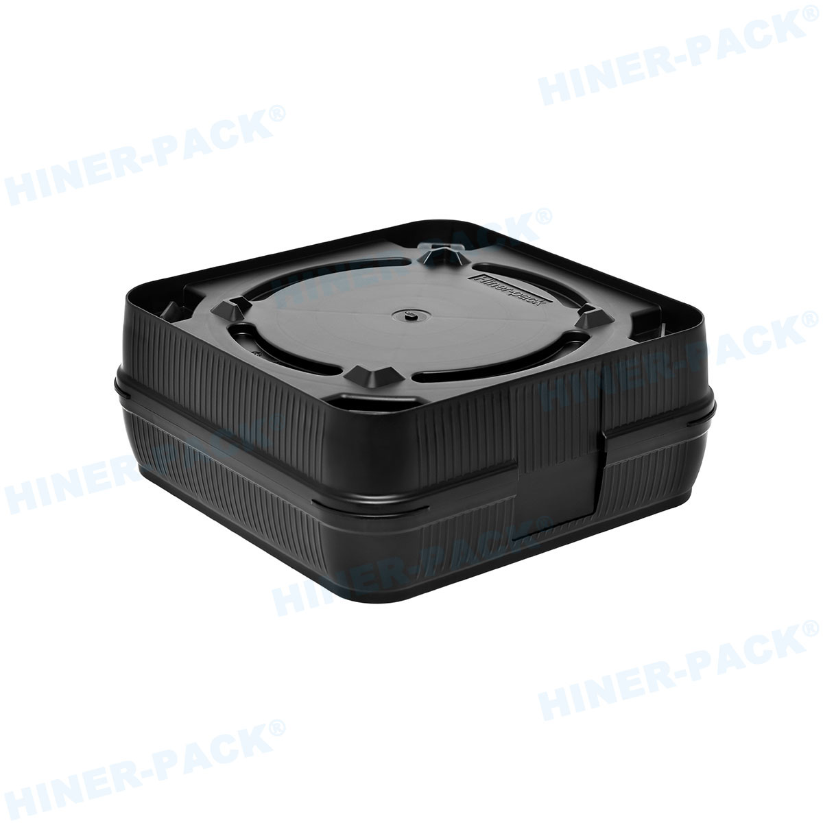
Material Selection and Polymer Performance in Wafer Packaging
The foundational layer of wafer protection rests on the raw polymers chosen for injection molding. Standard packaging plastics are inadequate for semiconductor-grade shipping containers because they often contain additives that migrate to the surface or degrade under mechanical stress. A specialized wafer box factory like Hiner-pack selects high-purity, engineering-grade polymers such as Polypropylene (PP), Polycarbonate (PC), and Polyetheretherketone (PEEK) to meet rigorous structural and chemical requirements.
Electrostatic Discharge Protection and Surface Resistivity
Silicon wafers are highly sensitive to electrostatic discharge (ESD) events, which can instantly vaporize sub-micron gate oxide layers. Untreated polymers easily build up static charges through friction during transport, a phenomenon known as triboelectric charging. To prevent this, the raw materials used in manufacturing wafer carriers must be engineered for static dissipation.
Carbon Powder and Fiber Fillers: Compounding polymers with specialized carbon blacks or carbon fibers creates a conductive network within the plastic matrix, allowing static charges to bleed off safely.
Surface Resistivity Ranges: The target surface resistivity for static dissipative wafer shippers is typically maintained between 105 and 1011 ohms per square, preventing both rapid discharges and static accumulation.
Inherently Dissipative Polymers (IDPs): For high-end applications where carbon sloughing (the shedding of carbon particles) is a concern, IDPs are integrated into the polymer blend to provide clean, non-sloughing ESD protection.
Selecting the appropriate additive balance requires deep material expertise, as excessive carbon loading can make the plastic brittle, leading to micro-cracking and particle generation during mechanical handling.
Outgassing and Airborne Molecular Contamination
Airborne Molecular Contamination (AMC) represents a silent threat to semiconductor yields. When wafer carriers are exposed to temperature fluctuations during shipping, the packaging materials can release volatile organic compounds (VOCs) through outgassing. These organic molecules deposit onto the exposed silicon surfaces, forming a thin carbon film that interferes with thin-film deposition, gate oxidation, and lithography steps.
To qualify materials for use, a reputable wafer box factory conducts testing in accordance with ASTM E595 standards. These tests measure Total Mass Loss (TML) and Collected Volatile Condensable Material (CVCM). Standard thresholds demand a TML of less than 1% and a CVCM of less than 0.1%. By utilizing high-purity Polycarbonate or low-outgassing Polypropylene grades, Hiner-pack ensures that chemical residues do not accumulate on wafers during long-term storage or international shipping.
Manufacturing Standards Inside a Wafer Box Factory
The performance of a wafer container is determined not only by its material composition but also by the environment in which it is molded, assembled, and packaged. A standard industrial plastic molding facility cannot meet the low particle limits required by the semiconductor sector. A specialized wafer box factory must operate dedicated cleanroom production lines to prevent ambient contamination.
Cleanroom Injection Molding and Automation
The injection molding process must occur within an environment classified under ISO 14644-1 standards, typically an ISO Class 5 or Class 6 cleanroom. Standard industrial air contains millions of particles per cubic meter; a cleanroom limits this count through High-Efficiency Particulate Air (HEPA) filtration and positive air pressure systems.
Automated Part Removal: Robotic arms are utilized to retrieve molded parts directly from the injection press, reducing human interaction, which is the primary source of sodium, potassium, and skin oil contamination.
Mold Venting and Maintenance: Injection molds are designed with advanced venting systems to prevent gas traps, which can cause micro-burns on the plastic surface, resulting in friable areas that shed particles over time.
Closed-Loop Material Feeding: Raw polymer pellets are fed to the molding machines through sealed, stainless steel vacuum systems to prevent exposure to ambient warehouse dust before melting.
By controlling these variables, the factory prevents microscopic particulates from becoming embedded in the plastic surface during the molten phase, where they would otherwise remain trapped until migrating onto a silicon wafer during transport.
Precision Dimensional Stability and Mechanical Tolerance
Modern semiconductor fabrication facilities rely heavily on Automated Material Handling Systems (AMHS) and robotic end-effectors to load and unload wafer cassettes. If a shipping box or process cassette exhibits dimensional deviation due to uneven thermal shrinkage during molding, the robotic sensors may misread the container position. This mismatch can result in edge chipping, scratching, or catastrophic wafer breakage.
To avoid these errors, a wafer box factory must maintain tight dimensional tolerances, often within +/- 0.1 mm, across high-volume production runs. Achieving this level of precision requires precise cooling channel design within the injection molds to prevent warpage, alongside real-time monitoring of injection pressure and barrel temperature. Compliance with SEMI (Semiconductor Equipment and Materials International) standards, such as SEMI M1 and SEMI E1.9, ensures that the external dimensions, latching mechanisms, and pocket spacing align perfectly with factory automation tools.
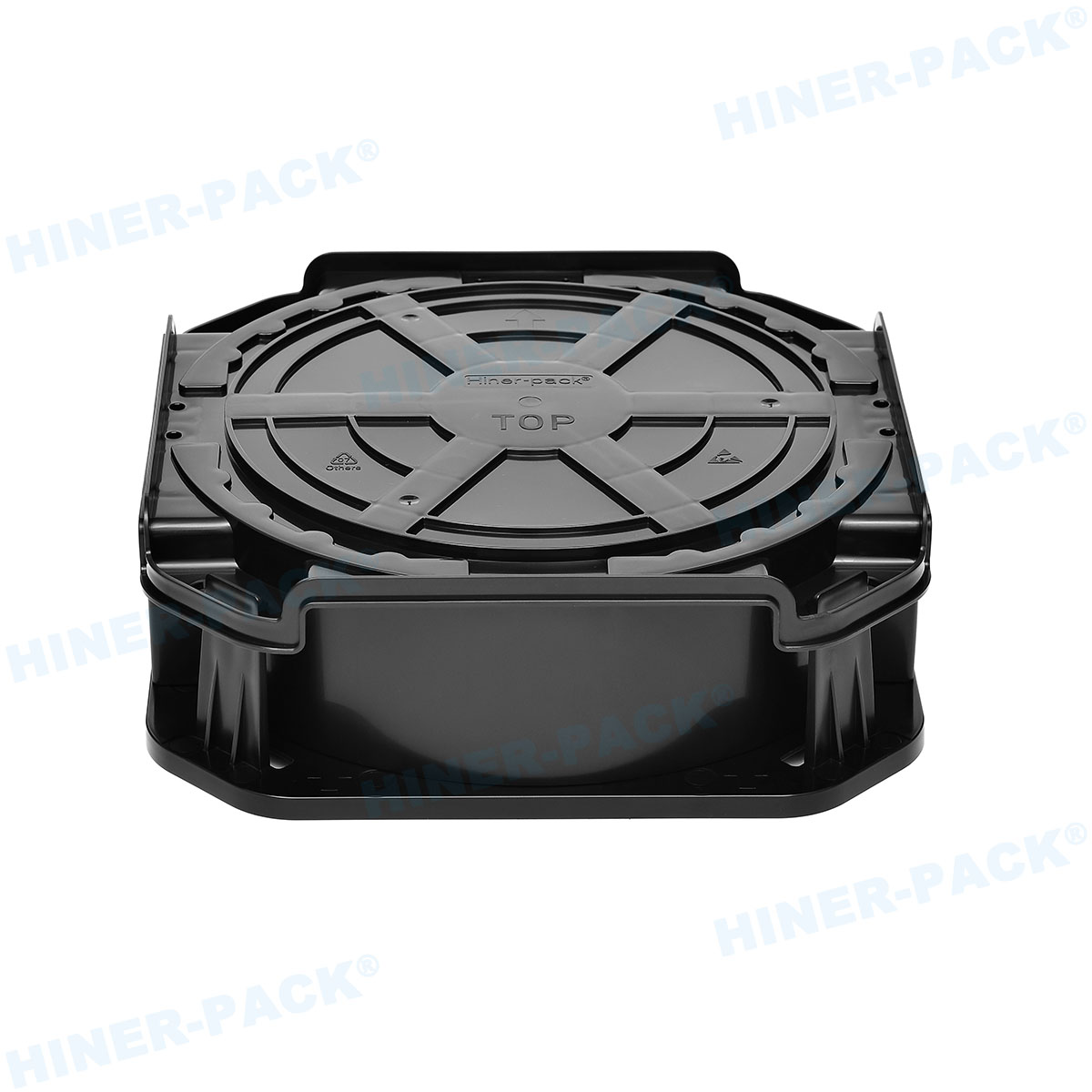
Industry Pain Points in Wafer Transport and Storage
Shippers and carriers must withstand a wide range of mechanical and environmental stresses during global logistics. Understanding these challenges allows engineering teams to design packaging that mitigates common field failures.
Vibration Resonance and Physical Micro-Damage
During truck or air transport, packaging is subjected to continuous low-frequency vibrations. If the internal supports or cushions of a wafer box do not match the resonance profile of the silicon wafers, the wafers can vibrate rapidly within their designated slots. This movement leads to structural wear, generating silicon dust that settles on the active circuitry.
To minimize vibration-induced damage, specialized wafer carriers use precision-designed retainers and cushions. These components are molded from soft, high-purity elastomers that absorb kinetic energy without transferring excessive localized pressure to the wafer edges. The tolerance between the wafer edge and the plastic guide rails must be calculated precisely to permit thermal expansion while preventing lateral rattling.
Moisture Ingress and Oxidation Control
Exposed silicon is highly reactive to atmospheric oxygen and moisture, which leads to the rapid growth of native oxide layers. This native oxide must be etched away prior to subsequent processing, adding manufacturing steps and increasing chemical usage. For patterned wafers awaiting assembly, moisture can initiate galvanic corrosion on aluminum or copper bond pads.
A professional wafer box factory addresses this by integrating robust sealing solutions into multi-wafer shipping boxes. Using elastomeric gaskets made of thermoplastic vulcanizates (TPV) or fluoropolymer rubbers, the containers maintain a hermetic seal. When combined with desiccant packs or nitrogen purging ports, these sealed containers keep the internal relative humidity below critical levels, safeguarding the wafers from chemical degradation during transoceanic shipping.
Engineering Solutions Provided by Hiner-pack
With years of experience in cleanroom packaging, Hiner-pack manufactures wafer transport systems designed to address these complex industry challenges. Our production facility integrates advanced polymer processing technologies with rigorous quality control protocols to supply reliable packaging solutions globally.
Our product portfolio includes single-wafer compact shippers, coin boxes, multi-wafer shipping boxes, and process cassettes compatible with standard wafer diameters, including 150mm, 200mm, and 300mm configurations. By sourcing high-purity raw materials and utilizing automated ISO Class 5 cleanroom molding lines, we deliver products that combine physical durability with minimal chemical outgassing.
To verify the cleanliness and physical integrity of every production lot, our quality control laboratory performs a suite of standard tests:
Liquid Particle Counting (LPC): Evaluates the level of extractable particulate contamination on carrier surfaces to ensure compatibility with high-yield manufacturing.
Ion Chromatography (IC): Detects trace levels of inorganic anions and cations, such as chloride, sulfate, and sodium, which can cause chemical staining on wafer surfaces.
Coordinate Measuring Machine (CMM) Inspection: Verifies critical dimensions against SEMI guidelines to guarantee compatibility with factory robotics and end-effectors.
Frequently Asked Questions
Q1: What standard quality certifications should a wafer box factory possess?
A1: A qualified factory should hold ISO 9001 certification for quality management systems and operate cleanroom manufacturing environments certified under ISO 14644-1 (typically ISO Class 5 or Class 6). For companies serving the automotive or medical semiconductor sectors, adherence to stricter quality tracking and material traceability protocols is also required to ensure long-term reliability.
Q2: Why is Polycarbonate preferred over standard Polypropylene for certain wafer shippers?
A2: Polycarbonate provides superior structural rigidity, impact resistance, and dimensional stability compared to Polypropylene. It is also transparent, allowing operators or automated vision systems to verify wafer presence and orientation without opening the container. However, Polypropylene remains a popular, cost-effective option for raw silicon wafer shipping where optical clarity is not required.
Q3: How does a wafer box factory prevent static buildup on transparent containers?
A3: To maintain transparency while achieving static dissipation, manufacturers utilize Inherently Dissipative Polymers (IDPs) or specialized transparent conductive coatings. These additives form a microscopic conductive network that dissipates static charges without relying on carbon black fillers, which would otherwise render the plastic opaque and introduce a source of particle shedding.
Q4: What is the purpose of a wafer cushion in a shipping box, and how is its cleanliness ensured?
A4: Wafer cushions or liners are placed at the top and bottom of wafer stacks to absorb shock and prevent vertical movement during shipping. To ensure cleanliness, these cushions are molded from high-purity elastomers, such as medical-grade silicone or specialized thermoplastic elastomers, which undergo hot-water extraction processes to remove residual plasticizers, catalysts, and surface contaminants before assembly.
Q5: How does Hiner-pack verify that its wafer boxes meet SEMI standards?
A5: Hiner-pack utilizes high-precision Coordinate Measuring Machines (CMM) and optical gaging systems to inspect the mechanical dimensions of each production batch. We compare these measurements directly against SEMI specifications, including latch interfaces, pocket pitch, and external alignment notches, ensuring seamless integration with automated fab machinery and robotic sorters.
In the highly competitive semiconductor manufacturing sector, even minor packaging deficiencies can lead to significant financial losses due to contamination or mechanical damage. Selecting a wafer box factory that prioritizes material purity, precise cleanroom molding, and rigorous dimensional verification is vital for protecting your high-value silicon wafers throughout global logistics networks.
For detailed product specifications, material safety datasheets, or to discuss customized engineering options for your specific wafer transport requirements, please contact our technical sales team for an inquiry.














