
In the semiconductor manufacturing value chain, the transit of processed and unprocessed silicon wafers represents a phase where yield is highly vulnerable. Once a wafer completes its lithographic, etching, and metallization steps, its accumulated value is substantial. Transporting these fragile structures between fabrication facilities, metrology labs, and packaging plants requires specialized containment systems. When procurement departments search for a suitable wafer box for sale, the decision-making process must extend far beyond basic dimensions and price points. The physical integrity and chemical purity of the enclosure directly impact final device yield.
Hiner-pack designs and manufactures high-performance wafer packaging solutions tailored to meet the strict demands of modern semiconductor logistics. Understanding the interaction between packaging materials, ambient contaminants, and mechanical forces is necessary to prevent micro-contamination, electrostatic damage, and physical breakage during shipping.
Material Science in Wafer Packaging: Managing ESD and Outgassing
The choice of polymer for a wafer shipper determines its protective capabilities. Standard consumer-grade plastics are entirely unsuitable for semiconductor environments due to the phenomena of triboelectric charging and chemical outgassing.
Electrostatic Discharge (ESD) Protection
Silicon wafers are highly sensitive to electrostatic discharge. During transport, sliding friction between the wafer and the carrier can generate thousands of volts of static electricity if non-dissipative materials are used. To prevent this, wafer containers must be molded from engineered polymers with controlled surface resistivity.
Conductive Materials: Surface resistivity ranging from 10^3 to 10^5 ohms/square. These materials allow charges to dissipate quickly, but can sometimes cause rapid discharge if a charged object contacts them.
Static Dissipative Materials: Surface resistivity between 10^6 and 10^9 ohms/square. This is the preferred range for most wafer contact areas, as it allows a controlled, safe decay of static charges without causing sudden discharge events.
Insulative Materials: Surface resistivity above 10^12 ohms/square. These are avoided for primary contact surfaces because they retain localized charges for extended periods, attracting airborne molecular contaminants (AMC) to the wafer surface.
Low Outgassing and Chemical Inertness
Volatile Organic Compounds (VOCs) emitted by low-grade plastics can condense onto the active surfaces of silicon wafers. This molecular contamination can degrade gate oxide integrity, alter surface hydrophobicity, and interfere with subsequent thin-film deposition steps. Consequently, high-purity polymers such as Polycarbonate (PC), Polypropylene (PP), and Polyetheretherketone (PEEK) are utilized. These polymers undergo rigorous testing, such as ASTM E595, to measure Total Mass Loss (TML) and Collected Volatile Condensable Material (CVCM). Hiner-pack utilizes virgin-grade resins with low outgassing profiles to ensure that the internal microenvironment of the container remains free of organic deposits.
Structural Design Variations of Modern Wafer Shippers
Depending on the wafer diameter, thickness, and transport volume, different structural configurations are required. Selecting a wafer box for sale requires matching the physical design to the specific logistics workflow.
Coin Boxes (Single Wafer Shippers)
For research and development, low-volume sampling, or the transport of highly specialized compound semiconductor substrates (such as Gallium Arsenide or Silicon Carbide), single wafer shippers, commonly known as coin boxes, are the industry standard. These containers consist of a base, a lid, and a spring-loaded retention insert. The design relies on a starburst-shaped spring or a silicone cushion that applies a gentle, uniform downward force on the center or perimeter of the wafer. This prevents vertical movement and lateral sliding, mitigating the danger of edge chipping.
Horizontal Wafer Shippers (Multi-Wafer Canisters)
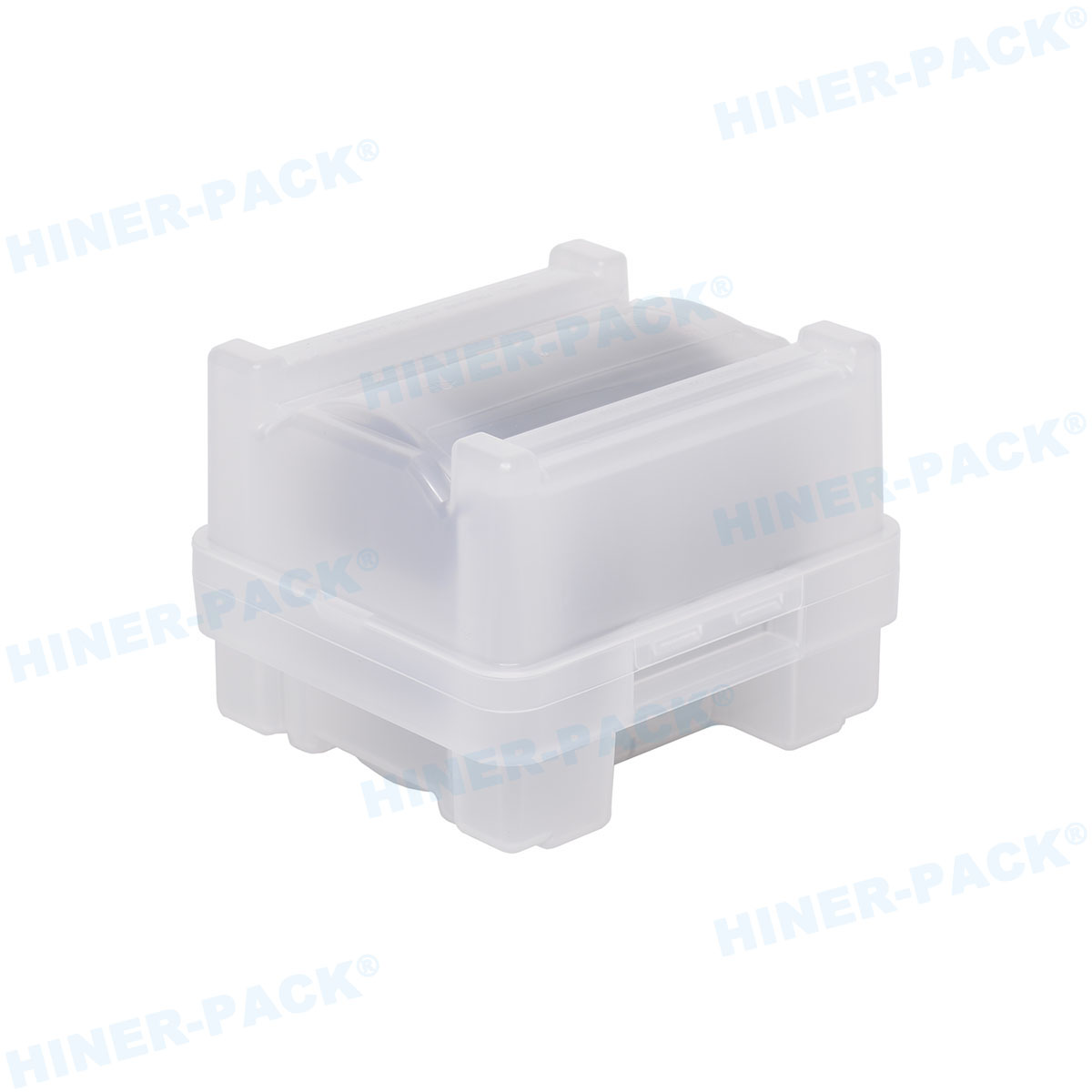
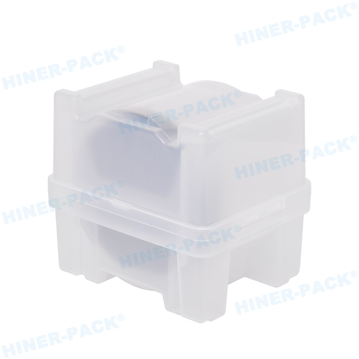
For larger volume shipments, typically containing 25 wafers, horizontal shippers are utilized. These systems feature internal slots that hold each wafer securely by its edges. The spacing between slots must be engineered to prevent wafer-to-wafer contact under severe deceleration forces. High-performance multi-wafer shippers feature integrated structural ribs on the outer shell to absorb external impacts, translating mechanical energy away from the internal cargo.
Contamination Control and Cleanroom Manufacturing Standards
A shipping container must not introduce the very contaminants it is designed to exclude. Therefore, the manufacturing environment of the packaging itself is a key quality differentiator.
Every wafer box manufactured by Hiner-pack is produced, assembled, and packed within an ISO Class 5 (Class 100) or ISO Class 6 cleanroom environment. This process control ensures that airborne particulate matter does not settle on the internal surfaces of the coin boxes or multi-wafer canisters prior to sealing. The molding machines are equipped with specialized HEPA filtration units, and the raw resin handling systems are closed-loop to prevent cross-contamination.
Following injection molding, the components undergo multi-stage deionized water washing processes to remove residual surface particles, ionic contaminants, and processing aids. After drying under ultra-pure nitrogen gas, the products are double-bagged in cleanroom-compatible, anti-static packaging to ensure they remain pristine until opened at the customer's facility.
Finding the Right Wafer Box for Sale for Your Fab Operations
Sourcing the appropriate shipping container requires a systematic analysis of your operational variables. Not all wafer shippers are designed for the same mechanical or thermal environments.
First, evaluate the wafer diameter and substrate thickness. Standard silicon wafers of 200mm and 300mm diameters have standardized thicknesses (typically 725 microns). However, thin wafers—often ground down to 100 microns or less for 3D packaging and stacked-die applications—require highly specialized support structures. Standard slot widths in general-purpose shippers allow too much vertical play for thin wafers, which can lead to micro-fractures during transit. Specialized thin-wafer shippers incorporate ultra-soft elastomeric liners that cradle the wafer edge without applying compressive stress.
Second, consider the automated material handling systems (AMHS) used within your facility. For automated fabs, the outer dimensions, registration notches, and robotic handling flanges of the wafer carrier must adhere strictly to SEMI standards. A minor deviation in the outer molding tolerances can cause mechanical misalignments in robotic transfer arms, leading to wafer breakage and tool downtime. Hiner-pack designs carriers with strict dimensional tolerances to ensure compatibility with standardized automated process equipment.
Handling the Physical Challenges of Cross-Border Shipping
Long-distance international shipping subjects semiconductor packaging to severe physical stresses, including vibration, shock, pressure changes, and temperature fluctuations.
During air freight, cargo holds can experience rapid depressurization and temperature drops. A sealed wafer box without pressure equalization can deform or crack due to pressure differentials. To counteract this, advanced shipping systems incorporate breathable, hydrophobic vent membranes. These membranes allow air pressure to equalize between the interior and exterior of the box while preventing the ingress of moisture, liquid water, and particulate matter.
Vibration during road transport can also induce resonance in silicon wafers. If the natural frequency of the wafer matches the vibration frequency of the transport vehicle, the resulting displacement can cause the wafers to strike the interior walls of the container, leading to micro-cracking. Hiner-pack addresses this by analyzing the damping characteristics of our polymer blends and incorporating vibration-absorbent elastomeric inserts that decouple the wafers from high-frequency transport vibrations.
Matching Wafer Materials with Appropriate Container Formulations
The rapid growth of compound semiconductors, such as Gallium Nitride (GaN) and Silicon Carbide (SiC) for power electronics, has introduced new packaging requirements. These alternative substrate materials are physically heavier and significantly more brittle than standard monocrystalline silicon.
When searching for a wafer box for sale to house compound semiconductor substrates, mechanical shock absorption is the primary design priority. Because these substrates are highly susceptible to cleavage along crystalline planes, any localized impact can cause catastrophic shattering. Hiner-pack provides customized coin boxes and horizontal carriers with specialized internal geometries that distribute holding pressure evenly across the perimeter, reducing localized stress concentrations.
A Systematic Approach to High-Volume Procurement
For high-volume semiconductor assembly and test (OSAT) facilities and foundries, consistency in packaging supply chains is necessary to maintain production continuity. Packaging must be treated as an extension of the cleanroom process itself. This requires working with a supplier capable of providing rigorous batch-to-batch consistency and comprehensive material traceability.
Hiner-pack implements a strict quality management system where every production batch is traceable back to the raw material resin lot. Regular testing for surface resistivity, dimensional stability, and particulate cleanliness is documented and provided to partners as part of our quality assurance commitment. Our global logistics network ensures that high-volume orders are fulfilled with predictable lead times, minimizing inventory holding costs for fabs.
Contact Hiner-pack for High-Performance Semiconductor Packaging
Securing your valuable semiconductor cargo requires packaging engineered to the highest cleanliness and mechanical protection standards. Hiner-pack offers a comprehensive range of wafer shippers, coin boxes, and customized carrier solutions designed to minimize yield loss due to contamination and physical damage.
To receive technical datasheets, material certificates, or a customized quotation for your specific wafer size and transport requirements, please contact our technical sales team directly. We are prepared to assist you in selecting and configuring the appropriate containment solution for your semiconductor manufacturing workflow.
Frequently Asked Questions
Q1: What materials are commonly used in wafer packaging to prevent ESD?
A1: High-quality wafer shippers are typically molded from engineered Polycarbonate (PC), Polypropylene (PP), or Polyethylene (PE) blended with carbon-filled or inherently dissipative additives. This modification achieves a controlled surface resistivity of 10^6 to 10^9 ohms/square, which safely dissipates static charges and prevents electrostatic discharge damage to sensitive integrated circuits.
Q2: How does outgassing from plastic shipping containers affect silicon wafers?
A2: When plastic containers outgas, they release volatile organic compounds (VOCs) that can condense on the exposed silicon wafer surfaces. This thin film of organic contamination can interfere with lithography, alter thin-film adhesion, and degrade gate oxide performance. Utilizing high-purity, low-outgassing polymers that comply with ASTM E595 standards prevents this type of molecular contamination.
Q3: What is the difference between a coin box and a horizontal wafer shipper?
A3: A coin box is designed to hold a single wafer securely using a vertical spring-loaded mechanism or elastomeric insert, making it ideal for R&D, sampling, and low-volume shipping. A horizontal wafer shipper, or canister, is designed to carry multiple wafers (typically 25) arranged horizontally in parallel slots, which is optimized for high-volume automated logistics.
Q4: How do cleanroom standards apply to the production of these shippers?
A4: To ensure that the containers do not introduce particulate contamination, they must be molded, cleaned, and packed in an ISO Class 5 or Class 6 cleanroom. The process includes washing the molded parts with deionized water and sealing them in double-layered anti-static bags to maintain cleanroom-level cleanliness during transit to the fab.
Q5: Can these containers be reused, or are they single-use only?
A5: While many wafer shippers are robust enough for multiple uses, reuse requires strict recleaning protocols in an ISO-certified cleanroom to remove accumulated particulates and chemical residues. For critical front-end wafer transit, single-use shipping is often preferred to completely eliminate the possibility of cross-contamination between different manufacturing facilities.














