
The global semiconductor supply chain requires silicon and compound wafers to travel thousands of miles between fabrication plants, testing facilities, and assembly sites. Throughout this transit process, delicate microstructures are exposed to dynamic mechanical forces, thermal variations, and environmental contaminants. At sub-nanometer nodes, even a sub-micron particle or a minor static discharge can compromise an entire batch of wafers, leading to severe yield losses. Consequently, the selection of a wafer box manufacturer is not merely a purchasing decision but a fundamental step in securing product yield and supply chain integrity.
Modern semiconductor logistics require transport systems that do more than simply hold a product. These systems must act as cleanroom-grade micro-environments that isolate wafers from external hazards. Hiner-pack designs high-precision wafer transport solutions engineered to meet the stringent standards of contemporary semiconductor packaging operations, ensuring that wafers arrive at their destination without degradation.
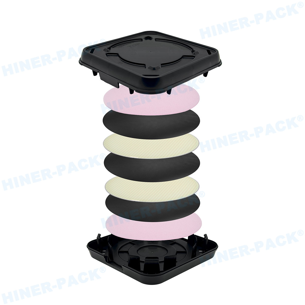
Understanding the Environmental Hazards of Wafer Transport
To evaluate a wafer box manufacturer, one must first analyze the physical and chemical forces that threaten wafer integrity during storage and global transit. These threats fall into three primary categories: electrical, chemical, and mechanical.
Electrostatic Discharge (ESD) and Triboelectric Charging
During transport, the relative motion between the wafer and the carrier can generate triboelectric charges. Silicon is highly sensitive to static electricity. If these charges build up on the surfaces of the container, they create a high electrostatic potential. When a discharge occurs, it can instantly destroy the thin oxide layers on the integrated circuits.
Furthermore, static charges on carrier surfaces act as particle magnets. Electrostatic attraction pulls airborne particulates toward the wafer surface, making subsequent cleaning steps incredibly difficult. A professional wafer box manufacturer addresses this by incorporating conductive or dissipative additives into the polymer matrix, ensuring a controlled path for charge decay.
Airborne Molecular Contamination (AMC) and Outgassing
Polymer materials naturally release volatile organic compounds (VOCs) over time, a process known as outgassing. In closed shipping containers, these molecules accumulate and deposit onto the active surfaces of the wafers. This organic contamination is particularly problematic during high-temperature fabrication processes, where the deposited carbon can cause defects in thin-film growth or photolithography patterning.
Mitigating AMC requires strict control over the raw materials. Manufacturers must use polymers that exhibit low outgassing characteristics, measured by Total Mass Loss (TML) and Collected Volatile Condensable Material (CVCM) standards, such as those defined by ASTM E595.
Mechanical Shocks, Vibration, and Substrate Stress
Transport vehicles subject shipments to continuous vibrational frequencies and sudden shock impulses. Wafers that have undergone backgrinding to reduce their thickness for 3D stacking or system-in-package (SiP) applications are exceptionally fragile. Micro-vibrations can cause the wafer edges to rub against the carrier slots, leading to micro-chipping, structural micro-cracks, or complete wafer breakage.
Material Science in Wafer Carrier Engineering
The core capability of any wafer box manufacturer lies in material formulation. Standard consumer-grade plastics are entirely unsuitable for semiconductor logistics. Instead, specialized engineering thermoplastics are utilized to achieve the necessary cleanliness, mechanical strength, and dimensional stability.
Polycarbonate (PC) and Modified Alloys
Polycarbonate is widely utilized for outer shipping boxes and secondary packaging due to its high impact resistance and structural rigidity. It provides a robust barrier against external physical impacts. When modified with anti-static additives, PC maintains its optical transparency, allowing operators or automated scanning systems to verify the contents of the container without opening it and exposing the interior to ambient air.
Polypropylene (PP) and High-Density Polyethylene (HDPE)
For internal cassettes or coin-style shippers where direct wafer contact occurs, modified polypropylene formulations are common. These materials offer excellent chemical resistance to acids and bases, making them suitable for wet processing environments as well as transport. High-purity PP formulations minimize the extraction of metallic impurities and anions, protecting the chemical purity of the silicon surface.
Advanced Fluoropolymers (PFA and PTFE)
In high-temperature or highly corrosive chemical environments, fluoropolymers like Perfluoroalkoxy (PFA) are selected. PFA resists thermal deformation and exhibits near-zero chemical reactivity. While more expensive, these materials are necessary for specific processing steps and high-end transport configurations where total chemical inertness is mandatory.
Comparison of Common Packaging Materials
Polycarbonate (PC): High impact strength, rigid, transparent; primarily used for outer enclosures and protective shells.
Polypropylene (PP): Good flexibility, low particle generation, chemical resistance; ideal for inner support structures and coin shippers.
Polyetheretherketone (PEEK): High thermal stability, minimal outgassing, high wear resistance; used for high-reliability contact points.
Manufacturing Cleanliness Standards and Quality Systems
An exceptional design is ineffective if the manufacturing environment introduces contamination during production. A reliable wafer box manufacturer must operate state-of-the-art cleanroom facilities to ensure that every container is pristine from the moment it is molded.
Cleanroom Injection Molding and Assembly
The injection molding process itself must be carefully controlled. Raw polymer pellets are fed into the molding machines via sealed, automated vacuum systems to prevent ambient dust contamination. The molding, assembly, inspection, and final packaging of the wafer boxes should occur in an ISO Class 5 (Class 100) or ISO Class 6 cleanroom environment.
In these controlled environments, high-efficiency particulate air (HEPA) filtration systems remove micro-particles from the air. Technicians wear full-body cleanroom suits to prevent human skin flakes or hair from contaminating the newly formed components. Continuous environmental monitoring tracks particle counts, relative humidity, and temperature to ensure production stability.
Ultra-Pure Water Washing Systems
Before packaging, molded components undergo multi-stage cleaning processes using Ultra-Pure Water (UPW). This water is filtered to remove particles down to the nanometer scale and deionized to eliminate trace minerals. The washing process removes any residual mold release agents, surface particles, or static charges, leaving the plastic surfaces completely clean.
Automation Compatibility and Dimensional Standards
Modern semiconductor fabrication facilities rely on Automated Material Handling Systems (AMHS). Robotic arms, overhead hoist transfers (OHT), and automated sorters handle wafer carriers continuously. A minute dimensional deviation can cause a mechanical jam, leading to system downtime or, worse, wafer destruction.
A precision wafer box manufacturer must adhere strictly to SEMI (Semiconductor Equipment and Materials International) standards. These standards dictate the precise dimensions, tolerance limits, and mechanical interfaces of wafer carriers, such as FOUPs (Front Opening Unified Pods) and FOSBs (Front Opening Shipping Boxes). High-precision metal molds and advanced quality control systems, including coordinate measuring machines (CMM), are used to verify that every critical dimension aligns with SEMI specifications.
Selecting a Custom Engineering Partner for Advanced Packaging
The rapid development of compound semiconductors, such as Silicon Carbide (SiC) and Gallium Nitride (GaN), has introduced new challenges for packaging. These wafers are often thicker, heavier, and more fragile than standard silicon substrates. Standard shipping boxes may not provide the precise fit required to prevent movement during transport.
In these scenarios, off-the-shelf solutions are often insufficient. A wafer box manufacturer must possess the engineering capability to design custom internal configurations, custom cushion layouts, and modified retaining rings. This process involves Finite Element Analysis (FEA) to simulate drop tests and vibration profiles, ensuring the custom design can absorb mechanical energy without transferring it to the delicate compound substrates.
Hiner-pack collaborates directly with semiconductor manufacturing teams to develop customized carrier designs. By matching the mechanical properties of the packaging to the specific weight, diameter, and brittleness of the substrate, engineered protection can be achieved for even the most non-standard wafer shapes and thicknesses.
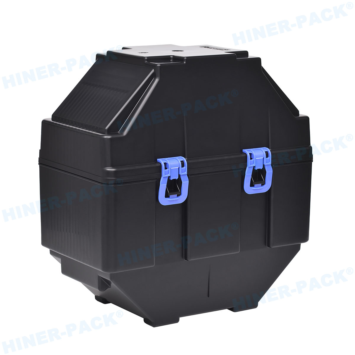
Structuring the Logistics Qualification Process
Qualifying a new packaging supplier involves a systematic evaluation process. Because the packaging directly impacts yield, semiconductor companies must perform rigorous testing before approving a new carrier for production volumes.
Material Characterization: Verifying surface resistivity, outgassing levels (TML/CVCM), and chemical purity using gas chromatography-mass spectrometry (GC-MS) and ion chromatography.
Dimensional Verification: Inspecting alignment pins, latching mechanisms, and robotic handling interfaces to confirm adherence to SEMI standards.
Dynamic Shipping Trials: Conducting real-world transport tests with dummy wafers equipped with accelerometers to measure vibration dampening and shock absorption.
Cleanroom Particulate Testing: Measuring particle transfer to dummy wafers before and after shipping trials to evaluate the wear resistance of the contact points.
Frequently Asked Questions
Q1: Why is surface resistivity so tightly controlled in wafer shipping containers?
A1: Surface resistivity determines how quickly an electrostatic charge decays. If the resistivity is too high, static charges remain on the plastic, attracting airborne particles and creating a discharge hazard. If it is too low, rapid discharges can occur, damaging delicate circuitry. Maintaining a range between 10^5 and 10^9 ohms per square ensures safe, controlled dissipation.
Q2: What is the main difference between polycarbonate and polypropylene wafer boxes?
A2: Polycarbonate is highly rigid, impact-resistant, and transparent, making it suitable for outer protective shells and automated handling boxes. Polypropylene is more flexible, offers excellent chemical resistance, and is typically used for inner cassettes, coin-style shippers, and process-oriented containers where contact with chemicals is common.
Q3: How does a wafer box manufacturer prevent outgassing?
A3: Outgassing is prevented by selecting ultra-pure, raw polymer grades that do not contain volatile additives, low-molecular-weight plasticizers, or unstable pigments. Additionally, the manufacturing process avoids contaminated lubricants, and finished parts are thoroughly cleaned and baked if necessary to drive off any residual volatiles.
Q4: Can wafer transport boxes be cleaned and reused in production?
A4: Yes, many shipping containers are designed for reuse within closed-loop logistics systems. However, they must undergo standardized, validated cleaning cycles using deionized water and specialized drying processes to ensure no micro-contamination remains from previous transit cycles.
Q5: How do compound semiconductor materials like SiC affect shipping box requirements?
A5: Silicon Carbide (SiC) and Gallium Nitride (GaN) wafers are denser, more brittle, and have different mechanical behaviors compared to silicon. They often require specialized shipping slots and internal cushion configurations designed to distribute pressure evenly and absorb high-frequency transport vibrations that could otherwise lead to edge chipping.
Inquire for Specifications and Custom Engineering Support
Securing semiconductor shipments requires a detailed understanding of material behavior, precision mechanics, and cleanroom disciplines. Hiner-pack manufactures high-purity wafer packaging solutions designed to shield sensitive substrates during international transit. For technical data sheets, dimensional drawings, or to discuss custom carrier designs for specialized wafer dimensions, please contact our engineering team to request a detailed consultation and evaluation samples.














