
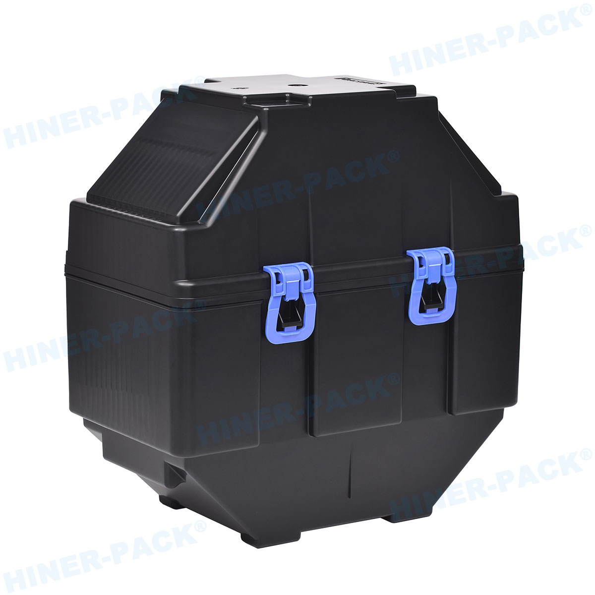
Semiconductor fabs require ultra-clean environments for wafer handling, storage, and transport. The containers that hold 300mm or 200mm wafers — FOUP (front opening unified pod), FOSB, and single-wafer shippers — are not simple plastic boxes. They are precision-engineered interfaces between wafer surfaces and the fab automation system. A reliable wafer container factory designs and produces carriers that meet SEMI E1.9, E15.1, and E57 specifications for particle generation, outgassing, and dimensional accuracy. This article examines the manufacturing processes, quality control methods, and material science decisions inside a professional wafer container factory.
Contamination control starts at the container level. Particles, metallic residues, or airborne molecular contaminants (AMCs) from the carrier can transfer to wafer surfaces, killing die yield. Moreover, electrostatic discharge (ESD) risks demand precise surface resistivity. Hiner-pack operates a dedicated cleanroom manufacturing line for wafer carriers, with injection molding, post-molding cleaning, and metrology all performed under ISO 5 (Class 100) conditions. Below, we outline the core competencies of a high-output wafer container factory and how each production step affects wafer protection.
Material Selection: Polycarbonate, PEEK, and Additives
Wafer containers are primarily injection-molded from polycarbonate (PC) or polyetheretherketone (PEEK), depending on temperature and chemical exposure. Key material properties include:
Low particle shedding – The compound must not generate microplastics under mechanical flexing or rubbing. Base resin with controlled melt flow index (MFI 10-20 g/10min).
Static dissipative range – Surface resistivity between 1×10⁵ and 1×10¹¹ ohms/sq. Achieved by adding carbon nanotubes or inherently dissipative polymers (IDP).
Low outgassing – Total outgassed organic compounds (TVOC) below 0.1 µg/cm² per SEMI E108. Avoid plasticizers and mold release agents.
Inside a wafer container factory, raw materials are stored in dry, filtered silos and vacuum-dried before molding to remove absorbed moisture. Polycarbonate absorbs 0.15-0.3% moisture which, if not removed, causes splay marks and internal stress — both particle sources. A reputable factory uses desiccant dryers with dew point below -40°C.
Injection Molding Process for Low-Stress Parts
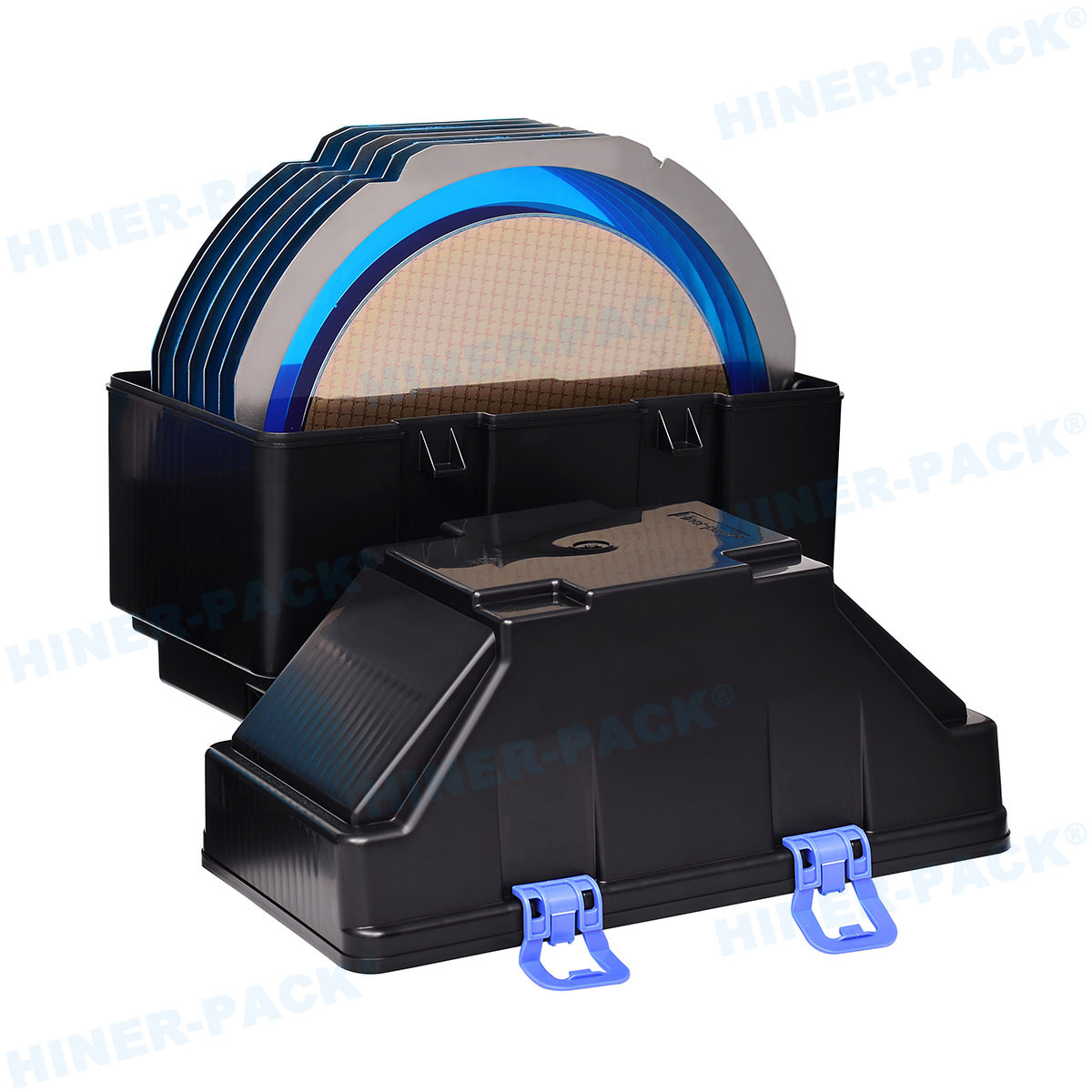
Wafer containers have thin walls (2-3 mm) and complex geometries: wafer supports (comb fingers), latching mechanisms, and robotic flange features. The molding process must eliminate flow marks, weld lines, and residual stress. Critical parameters:
Melt temperature – 280-320°C for PC; 380-400°C for PEEK. Too low causes short shots; too high degrades the polymer, releasing volatiles.
Mold temperature – 80-120°C via oil circulation. Uniform temperature distribution prevents differential shrinkage that warps the pod door flange.
Injection speed and pressure – multistage profiles with slow speed through the gate to avoid jetting, followed by fast fill to reduce weld lines.
Holding pressure – optimized to avoid sink marks while keeping part density uniform (target specific gravity 1.19-1.21 for PC).
A wafer container factory like Hiner-pack uses electric injection molding machines (Toyo, Fanuc) with closed-loop control. Each cavity is validated via mold flow simulation. After demolding, parts are automatically degated and sent to a cleanroom for deflashing — any flash (thin excess plastic) will generate particles during wafer loading.
Post-Molding Operations and Cleanroom Assembly
Molded parts (container shell, door, wafer cushions, front labels) are washed in a multi-stage DI water ultrasonic bath (60°C, 40 kHz) to remove mold release, fingerprints, and loose particles. Drying occurs in a Class 10 HEPA-filtered oven at 50°C. Assembly of the FOUP includes:
Inserting the seal (silicone or TPE gasket) into the door groove — gasket must be plasma-treated for adhesion.
Installing the front latch mechanism with stainless steel springs and cams (no lubricants).
Attaching the RFID tag (for fab tracking) and the robotic handling flange.
Installing the purge ports with check valves (for nitrogen purge during storage).
The entire assembly line operates under ISO 3 (Class 1) cleanroom conditions, with operators wearing bunny suits and using HEPA-filtered workstations. Every assembled container undergoes a particle count test: a clean cassette is placed inside and agitated for 5 minutes, then airborne particles ≥0.1 µm are measured. A passing container yields < 10 particles/ft³ inside its cavity — 10× cleaner than the fab minienvironment requirement.
Wafer Contact Surface Engineering
The wafer supports (also called contact points or comb fingers) are the only surfaces that touch the wafer edge and backside. Their design determines particle generation during loading/unloading. Advanced wafer container factory solutions incorporate:
Point contact geometry – radius of curvature 0.5-1.0 mm, polished to mirror finish (Ra < 0.2 µm) to minimize friction.
Softlanding features – flexible finger designs made of PEEK or polyethersulfone (PES) that deflect slightly when the wafer is placed, absorbing kinetic energy.
Anti-rotation ribs – vertical ribs on the finger side prevent lateral sliding but never contact the active die area.
Each batch of containers is tested on a wafer handling simulator: a 300mm test wafer is inserted and removed 1000 times, then the wafer is inspected for scratch marks and particle adders (increase > 5 particles ≥0.2 µm per wafer pass is cause for rejection).
Quality Assurance Protocols in a Wafer Container Factory
To meet the requirements of semiconductor fabs (e.g., TSMC, Intel, Samsung), a wafer container factory must maintain several metrology stations:
Dimensional measurement – using CMM (coordinate measuring machine) to verify SEMI E1.9 standard: pocket pitch tolerance ±0.1 mm, door opening flatness < 0.2 mm.
ESD surface resistivity – measured at 23°C, 50% RH with concentric ring probes per ANSI/ESD STM11.11. The container must show consistency across all interior surfaces.
Outgassing analysis – headspace GC-MS (gas chromatography–mass spectrometry) after heating the container to 80°C. Limits: siloxanes < 0.05 ppb, amides < 0.1 ppb.
Seal leak rate – the closed container is pressurized to 100 Pa differential and leak rate measured with a mass flow meter. FOUPs must hold at least 95% of pressure after 60 seconds.
Cross-contamination test – aluminum or copper witness coupons placed inside the container for 72 hours, then analyzed by TXRF (total reflection X-ray fluorescence) for metal residues (Fe, Cu, Al < 1×10¹⁰ atoms/cm²).
All data is logged and traceable by serial number. Hiner-pack provides a Certificate of Analysis with every shipment, summarizing five test results per batch.
Industry Pain Points and Solutions from the Container Manufacturing Perspective
Through years of supporting wafer fabs, five recurring issues have been identified in container performance. A specialized wafer container factory addresses each with design or process changes.
Pain Point 1: Particle Adders After 200+ Automation Cycles
Early wear of the door latch or hinge generates microscopic plastic debris inside the pod. Solution: Use metal-free, self-lubricating hinge materials (e.g., Torlon PAI) and apply a dry film lubricant (DLC or PTFE) that does not outgas. Also, design the latch to move in a linear rather than rotating path, reducing contact stress.
Pain Point 2: Wafer Breakage Due to Incorrect Finger Alignment
Misalignment of the container’s internal supports relative to the fab’s load port causes wafer edge chipping. Solution: Mold indexed alignment pins on the container base, and use automated optical inspection (AOI) to verify finger position within ±0.05 mm before assembly.
Pain Point 3: Moisture Ingress During Purge Storage
Even with a silicone seal, humidity can diffuse inside the FOUP, causing corrosion on moisture-sensitive wafers (e.g., copper interconnects). Solution: Install a desiccant cassette inside the container, or use a double-seal design with an intermediate chamber that is vacuum-evacuated before wafer insertion. Some wafer container factory units now offer integrated humidity sensors and RFID-based moisture logging.
Pain Point 4: Incompatibility with Different OHT (Overhead Hoist Transport) Systems
Different fabs use varying flange geometries. A container not matched to the OHT gripper can fall during transport. Solution: Design the top flange as a replaceable module. The factory can supply flanges meeting SEMI E15.1, E57, or customer-specific drawings.
Pain Point 5: Outgassing of Phthalates or Halogens
Some recycled plastics contain flame retardants that corrode aluminum wiring on wafers. Solution: A certified wafer container factory uses only virgin, halogen-free compounds and performs ion chromatography on each resin batch to ensure chloride < 1 ppm, bromide < 0.5 ppm.
Customization and Engineering Services
Beyond standard 300mm FOUPs (13-slot or 25-slot), wafer container factories also produce:
FOSB (front opening shipping box) – for wafer transport between fabs. Requires stronger wall construction and shock-absorbing foam inserts.
Single-wafer shippers – for prototype or high-value wafer transport. Materials include anti-static PETG with vacuum-sealed inner bags.
200mm wafer cassettes (open cassettes) – made of PFA or PVDF for wet process stations. These need chemical resistance and low extractables.
Custom reticle pods – for photomask storage, with ultra-low outgassing and precision cushioning.
Hiner-pack works directly with fab automation engineers to modify existing tooling for custom features: additional alignment pins, color-coded door handles for process differentiation, or embedded RFID with higher memory capacity. Lead times for custom mold modifications range from 12-16 weeks, including sampling and qualification in a customer’s load port.
Cleanroom Packaging and Shipping Requirements
Every wafer container leaving the factory must be double-bagged in nitrogen-purged ESD shielding bags. The outer packaging is a rigid corrugated box with foam padding to prevent compression of the door seal during transit. Shipping validation includes vibration testing (ISTA 3A) and drop testing from 30 cm onto concrete. The factory also provides a certificate of sterilization if required (gamma irradiation at 25-40 kGy, which may affect mechanical properties — polycarbonate turns yellow, PEEK retains properties).
Upon arrival at the fab, the container is wiped with IPA and vacuumed before entering the front opening unified pod (FOUP) stocker. A wafer container factory can provide incoming inspection instructions to the customer’s QA team.
Compliance and Certification Landscape
Wafer containers intended for international semiconductor supply chains must carry SEMI S2 (safety), SEMI S8 (ergonomics), and RoHS 3 certifications. Additionally, the factory’s quality management system should be ISO 9001:2015 and IATF 16949 (automotive-grade) for high-reliability metrics. Cleanroom manufacturing areas are certified to ISO 14644-1 Class 5 or better.
For export to European fabs, REACH SVHC compliance is required — all polymer additives must be declared and below 0.1% w/w. Hiner-pack maintains a restricted substances list (RSL) that is updated quarterly.
Frequently Asked Questions – Wafer Container Factory and FOUP Specifications
Q1: What is the difference between a FOUP and a FOSB produced by a wafer container factory?
Q2: How does a wafer container factory control particle generation from the container interior?
Q3: Can a wafer container factory produce non-standard slot pitches for thin wafers (e.g., 100 µm thickness)?
Q4: What is the acceptable surface resistivity range for ESD-safe wafer containers?
Q5: How often should wafer containers be recertified?
Q6: Are there wafer container factories that provide RFID-integrated tracking?
Engineering Support for Wafer Carrier Programs
For fab integration, custom container dimensions, or qualification samples from a certified wafer container factory, submit your request to Hiner-pack. Provide wafer diameter, desired slot count, automation interface type (OHT, AGV, or manual load port), and any special material requirements (high-temperature, UV resistance). The engineering team returns a detailed specification sheet and sample delivery schedule.
Inquiry channel: https://www.waferboxes.com/contact.html – Include project name, target quantity, and preferred certification standards (SEMI, RoHS, REACH).


