
Silicon substrates, ranging from traditional logic nodes to advanced compound semiconductors like Silicon Carbide (SiC) and Gallium Nitride (GaN), represent immense monetary and intellectual value. Transporting these highly sensitive substrates between front-end foundries, testing facilities, and outsourced semiconductor assembly and test (OSAT) centers requires an environment completely isolated from mechanical shock, particulate contamination, and static electricity. Engaging a qualified wafer boxes supplier involves rigorous evaluation of polymer science, cleanroom processing capabilities, and structural geometry. Sourcing teams must look past basic plastic molding parameters and demand scientifically validated packaging infrastructure to maintain maximum wafer yield during global transit.
Polymer Science: Electrostatic Discharge and Outgassing Dynamics
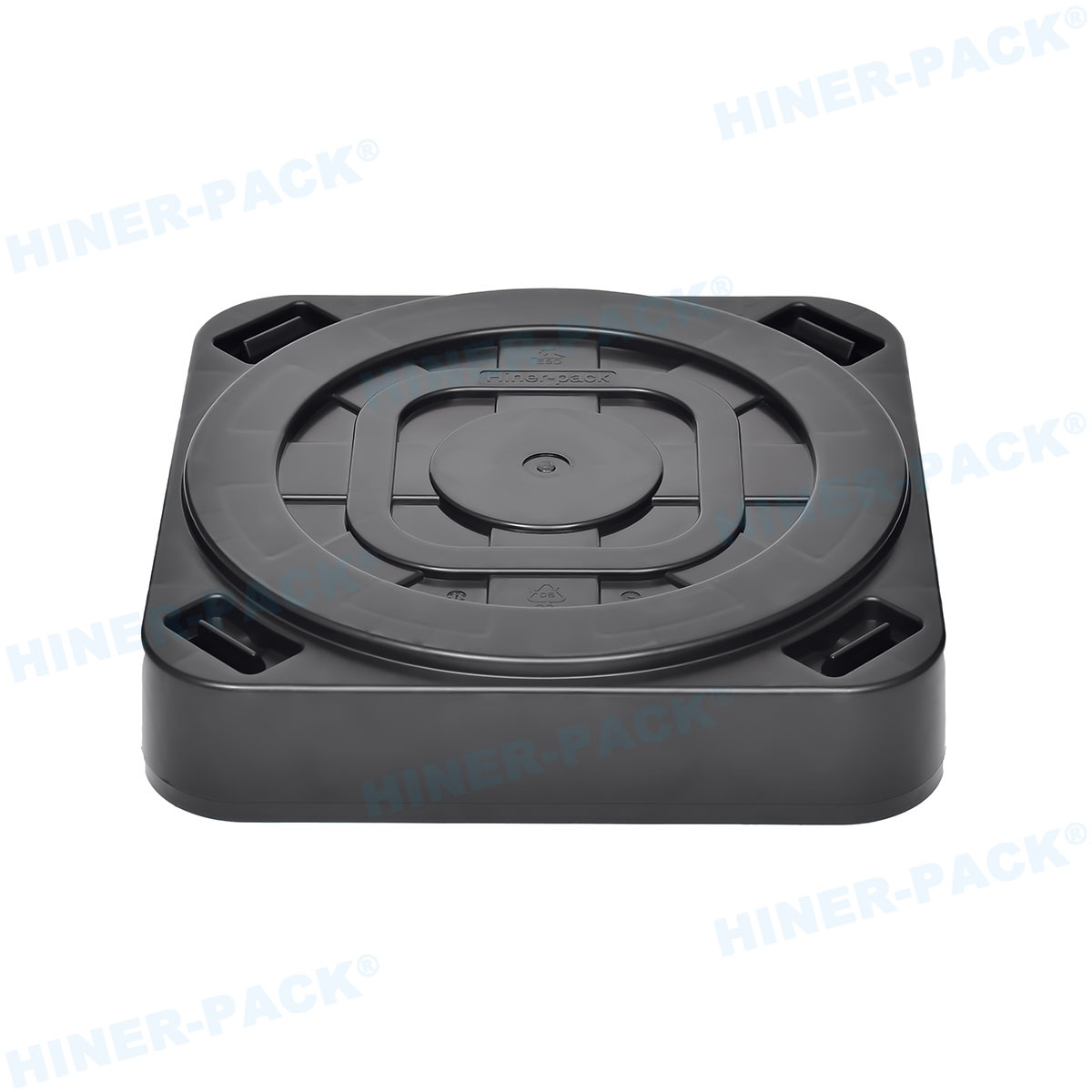
Silicon dioxide layers and microscopic circuit architectures are highly susceptible to electrostatic discharge (ESD). A sudden micro-spark can punch through a gate oxide layer, rendering an entire die non-functional. To prevent this sudden transfer of electrons, shipping containers must be engineered from highly specialized, blended polymers.
Standard commercial plastics act as insulators, accumulating static charges generated by friction during transit. An engineered carrier utilizes carbon-loaded polypropylene (PP) or advanced polycarbonate (PC) formulations to achieve a specific surface resistivity. This metric typically falls within the static-dissipative range of 10^5 to 10^9 ohms per square. This exact resistance profile allows any accumulated static charge to bleed off slowly and safely, rather than discharging rapidly into the silicon substrate. Top-tier manufacturers blend intrinsically dissipative polymers (IDPs) directly into the resin, ensuring the anti-static properties remain permanent and do not generate black carbon dust over time.
Volatile organic compounds (VOCs) present a secondary chemical parameter that requires strict monitoring. Cheaply manufactured plastics undergo a process known as outgassing, where chemical vapors are released from the polymer matrix as the material ages. In a sealed shipping box, these vapors deposit directly onto the pristine surface of the wafer, altering its surface energy and disrupting subsequent deposition or photolithography steps. High-purity materials must be specified to ensure near-zero outgassing, maintaining the exact chemical integrity of the semiconductor surface from the factory to the destination.
Categorizing Dimensional Requirements: From 4-Inch to 12-Inch Geometries
Different stages of semiconductor manufacturing dictate varying packaging geometries and volume capacities. A professional wafer boxes supplier maintains distinct product lines to accommodate the complete spectrum of substrate diameters, thicknesses, and automation requirements.
12-inch Wafer Shippers: The 300mm format represents the industry standard for high-volume logic and memory manufacturing. These large containers, often configured as Front Opening Shipping Boxes (FOSB) or Front Opening Unified Pods (FOUP), require massive structural rigidity. The plastic shell cannot flex or bow, as any dimensional distortion would prevent the automated robotic end-effectors inside the fab from extracting the wafers accurately.
8-inch Wafer Shippers: The 200mm diameter remains heavily utilized for analog devices, power electronics, and Micro-Electromechanical Systems (MEMS) manufacturing. These cassettes must provide precise wafer-to-wafer pitch spacing to prevent edge chipping during automated handling and wafer transfer operations.
6-inch Wafer Shippers: Widely used in the transition phase of power electronics and specialized radio frequency (RF) components. Shippers in this category often need to accommodate varying wafer thicknesses, particularly when dealing with thinned wafers requiring the Taiko back-grinding process.
4-inch Wafer Shippers: Smaller diameters are experiencing a massive production resurgence due to the rapid growth of compound semiconductors. SiC and GaN wafers are incredibly dense, expensive, and often more brittle than standard silicon. Shippers designed for these dimensions frequently utilize single-wafer configurations or specialized coin-roll formats with Tyvek interleaf paper to absorb microscopic vibrations.
Thermal Resilience: Engineering the Metal Carrier Series
Certain semiconductor fabrication steps require exposing the substrates to extreme thermal environments or aggressive chemical baths that standard polymer materials cannot survive. Processes such as high-temperature baking, chemical vapor deposition (CVD) pre-cleaning, or aggressive solvent washing necessitate an entirely different class of material containment.
The Metal Carrier Series addresses these extreme environmental parameters perfectly. Constructed from aviation-grade aluminum alloys, titanium, or high-purity 316L stainless steel, these cassettes maintain precise dimensional stability under immense heat. Metal carriers do not warp, melt, or release chemical vapors when subjected to bake-out ovens operating at several hundred degrees Celsius. The dimensional pitch between the slots remains perfectly parallel, ensuring the wafers do not bind or crack during thermal expansion.
The surface finish of these metal carriers undergoes electrochemical polishing to eliminate microscopic burrs or porous cavities where chemical residue could accumulate. This smooth, passivated surface ensures that the metal carrier itself does not become a source of particulate generation when submerged in ultrasonic cleaning tanks or concentrated acid baths. For highly specific chemical etching environments, these metal carriers can be coated with Perfluoroalkoxy alkanes (PFA) to provide ultimate chemical inertness while maintaining the structural rigidity of the underlying metal frame.
Cleanroom Manufacturing and Particulate Decontamination
Producing an ESD-safe molded container represents only half the manufacturing equation. The physical cleanliness of the container upon delivery dictates its usability inside an active wafer fab. A microscopic dust particle landing on a photolithography mask acts like a physical boulder, creating severe yield reduction across the integrated circuit layout.
The injection molding, robotic extraction, and final assembly processes must take place within a highly isolated environment. An established wafer boxes supplier processes their molded components inside certified ISO Class 4 or Class 5 cleanrooms. The HVAC systems in these facilities utilize heavy HEPA and ULPA filtration to continuously sweep airborne particulates away from the production lines.
Before the shipping boxes are fully assembled, the individual plastic components undergo a multi-stage decontamination wash. Technicians submerge the parts in heated, ultra-pure deionized (DI) water combined with ultrasonic agitation to knock loose any residual mold release agents or microscopic plastic shavings. Following forced-air drying under positive pressure filtration, the boxes are immediately vacuum-sealed in moisture-barrier, anti-static polyethylene bags. This rigorous protocol ensures that the receiving fab acquires a product that can be passed directly through the material airlock without requiring a secondary, costly decontamination wash onsite.
Mechanical Structural Integrity and Vibration Damping
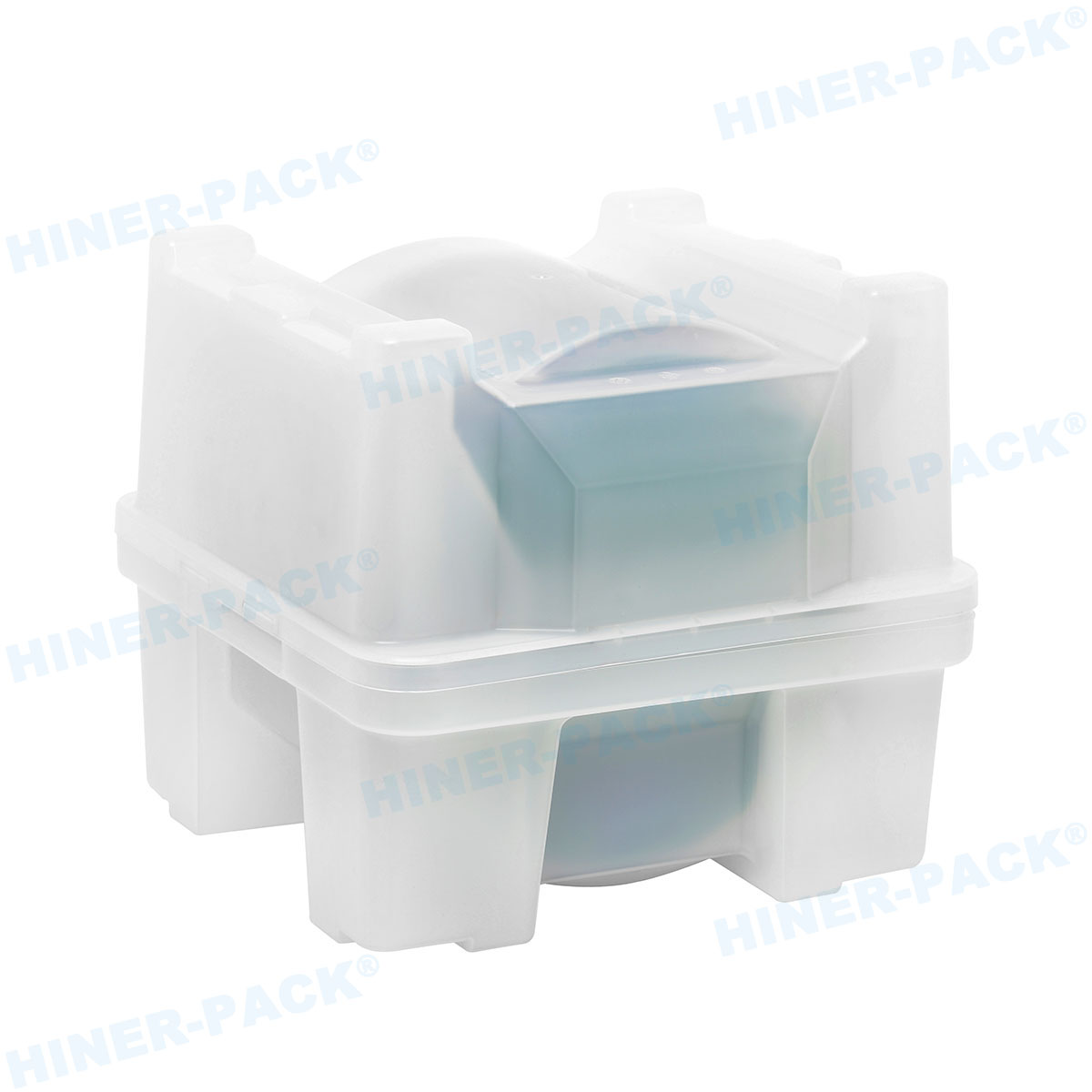
Global semiconductor supply chains require wafers to cross oceans via air freight and travel hundreds of miles on heavy transport trucks. This transit profile subjects the brittle silicon to constant low-frequency vibrations and the potential for sudden mechanical shocks during loading and unloading procedures.
The internal geometry of a single wafer shipper incorporates specialized cushioning mechanisms. Polyurethane foam rings or conical polymer springs press gently against the top surface of the wafer. This downward pressure immobilizes the substrate, preventing it from rattling against the hard plastic casing. The tension of these springs is precisely calibrated; it must be strong enough to hold the wafer in place, but gentle enough to avoid applying localized pressure points that could cause a micro-fracture.
The exterior shell features reinforced structural ribs designed to absorb the kinetic energy of an accidental drop. These designs are validated using International Safe Transit Association (ISTA) drop test protocols. If a logistics technician accidentally knocks the box off a workstation, the outer shell is engineered to flex and absorb the impact energy, rather than transferring that physical shockwave directly to the crystalline structure of the wafer inside.
Frequently Asked Questions
Q1: Why is surface resistivity measured in ohms per
square?
A1: This metric quantifies the electrical
resistance of a two-dimensional surface. In semiconductor packaging, maintaining
a range between 10^5 and 10^9 ohms per square ensures the material dissipates
static charges slowly enough to avoid a sudden arc, but fast enough to prevent
charge accumulation on the polymer surface.
Q2: Can standard polycarbonate be used if it is coated with an
anti-static spray?
A2: Topical anti-static sprays
are completely unacceptable in semiconductor manufacturing. These sprays wear
off through physical friction and introduce severe chemical contamination to the
cleanroom environment. The ESD properties must be compounded directly into the
polymer resin before the injection molding process begins.
Q3: What distinguishes a coin roll shipper from a single wafer
shipper?
A3: A coin roll shipper stacks multiple
wafers horizontally (resembling a roll of coins) separated by cleanroom-grade
Tyvek interleaf paper to absorb vibration. This maximizes shipping density for
bulk orders. A single shipper isolates one individual wafer in a dedicated
cavity, primarily used for highly sensitive R&D substrates or post-bumped
wafers.
Q4: How does a factory ensure dimensional accuracy for 12-inch wafer
shippers?
A4: Manufacturers utilize high-tonnage
precision injection molding machines and constantly monitor the mold temperature
to prevent plastic shrinkage during cooling. Dimensional accuracy is verified
using Coordinate Measuring Machines (CMM) to ensure the robotic handlers in the
fab can interface with the box seamlessly without causing wafer jams.
Q5: Why are specific shippers required for Silicon Carbide (SiC)
wafers?
A5: SiC wafers possess different physical
properties than standard silicon; they are denser, heavier, and extremely
expensive. Shippers designed for SiC require tighter internal tolerances,
enhanced compression springs, and stronger exterior ribbing to prevent edge
chipping during transit.
B2B Sourcing and Manufacturing Capabilities
Protecting the integrity of a semiconductor supply chain begins with fail-proof containment architecture. As a professional wafer boxes supplier, Hiner-pack engineers precision shipping solutions utilizing premium conductive polymers, rigorous mechanical drop testing, and strict cleanroom processing protocols. Our manufacturing facilities are equipped to produce the full dimensional spectrum, from 4-inch Wafer Shippers designed for emerging compound substrates up to massive 12-inch Wafer Shippers engineered for high-volume logic fabs. Incorporating our Metal Carrier Series provides reliable substrate handling during extreme thermal processing steps. Submit your exact dimensional requirements, ESD specifications, and volume projections to the engineering team at Hiner-pack today to receive detailed material data sheets and arrange for cleanroom-certified prototyping.














