
Semiconductor manufacturing requires high precision, where even microscopic contamination can affect production yields. During the transport of high-value silicon wafers between fabrication facilities, packaging plants, and end customers, protective packaging serves as a primary shield. Procurement managers and packaging engineers must evaluate a variety of shipping systems, ranging from single-wafer coin shippers to multi-capacity horizontal wafer shippers. Acquiring a comprehensive wafer box quotation involves assessing physical requirements, cleanroom manufacturing standards, and chemical compatibility to ensure secure transit.
For specialized suppliers like Hiner-pack, drafting an accurate proposal requires a deep understanding of the operational environment where these shippers will be deployed. Unit costs alone do not represent the total cost of ownership. Instead, factors such as polymer purity, electrostatic discharge protection, structural integrity under mechanical stress, and cleanroom packaging protocols collectively shape the final pricing structure. Examining these elements systematically allows semiconductor firms to manage logistics expenses while maintaining strict yield preservation protocols.
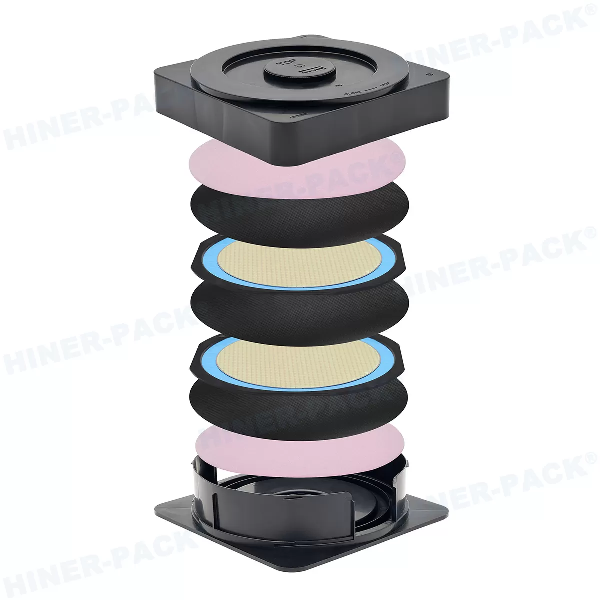
Primary Factors Influencing Your Wafer Box Quotation
When reviewing a wafer box quotation, the engineering specifications of the raw materials represent the largest cost driver. Different semiconductor processes demand specific polymer formulations to prevent chemical outgassing and electrostatic damage.
Polymer Grade and Chemical Purity
The choice of base resin directly dictates the performance and pricing of wafer transport containers. Lower-cost shipping options often utilize standard polypropylene (PP), which provides adequate physical impact protection but may not meet the outgassing requirements of front-end-of-line (FEOL) wafers. For more demanding cleanroom applications, high-purity polycarbonate (PC) or polybutylene terephthalate (PBT) is selected for its superior dimensional stability and low outgassing profile. Polycarbonate offers high transparency, allowing automated optical inspection systems to verify wafer presence without opening the protective enclosure, which reduces exposure to airborne particles.
In specialized applications, such as high-temperature processing or chemical-resistant transport, engineering polymers like PEEK (Polyetheretherketone) may be required for internal cassette components. Because raw polymer pricing fluctuates based on global chemical markets and purification steps, the base material selection remains a primary variable in any formal price breakdown.
Electrostatic Discharge (ESD) Protection Engineering
Electrostatic discharge represents a major vulnerability to microelectronic circuits. Wafer shippers must dissipate static charges safely to prevent electrostatic attraction of airborne particulates and direct ESD damage to active wafer circuitry. The methods used to achieve static dissipation significantly impact manufacturing complexity and raw material costs:
Carbon-Filled Conductive Materials: Integrating carbon powder or carbon fibers into the polymer matrix creates a reliable path for static charge dissipation. While cost-effective, standard carbon-filled resins can shed microscopic carbon particles over time, requiring strict validation processes.
Inherently Dissipative Polymers (IDP): These advanced compounds provide permanent static dissipation without the particulate shedding associated with carbon fillers. IDPs maintain cleanroom compatibility but require a higher initial investment, which is reflected in the product pricing.
Anti-Static Surface Treatments: Surface coatings offer temporary electrostatic protection for less sensitive shipping applications, providing a lower-cost alternative when long-term reuse is not planned.
A comprehensive wafer box quotation from Hiner-pack will typically specify the surface resistivity range (typically between 10^5 and 10^11 ohms per square) and the corresponding material classification to help procurement teams choose the appropriate protection level.
Structural Engineering and Wafer Dimensions
The physical dimensions and structural design of the shipping container must match the specific wafers being transported. The pricing structure varies according to the wafer size (typically 100mm, 150mm, 200mm, or 300mm) and the payload capacity of the container.
Standardized horizontal wafer shippers are designed to carry 25 wafers securely. These systems rely on precision-molded internal tracks and retention springs to minimize wafer movement during transit. The complexity of these internal components influences tool wear and injection molding cycle times during production, which affects the base manufacturing cost.
For single-wafer shipping requirements, coin-style shippers provide a compact solution. These containers utilize a screw-on or snap-fit lid combined with internal elastomeric liners or silicone cushions to hold the wafer securely in place. The manufacturing of these liners requires medical-grade, low-outgassing elastomers to prevent chemical residue from transferring to the wafer surface. Consequently, a customized wafer box quotation will detail the material specifications of both the outer shell and the internal retention elements to ensure full material traceability.
Cleanroom Manufacturing and Packaging Standards
The environment in which wafer shippers are molded, cleaned, and packaged is a key factor in pricing. Standard injection molding facilities cannot meet the low-particle requirements of the semiconductor industry. High-purity wafer packaging must be manufactured in controlled cleanrooms certified to ISO standards.
To achieve the required cleanliness, molded parts undergo multi-stage cleaning processes utilizing deionized (DI) water systems with a resistivity of 18.2 Megohm-cm. This cleaning step removes trace organic residues, ionic contaminants, and surface microparticles. Following purification, the shippers are dried using heated nitrogen gas within an ISO Class 4 or Class 5 environment.
The packaging of the shipping containers themselves is also highly regulated. To maintain cleanliness during transport to the customer's fabrication facility, products are double-bagged or triple-bagged in certified ultra-clean, low-density polyethylene (LDPE) cleanroom bags under vacuum. The cost of maintaining cleanroom infrastructure, operating ultrapure water filtration systems, and executing cleanroom packaging protocols represents a significant portion of the production cost listed on a wafer box quotation.
Logistics and Supply Chain Factors
Understanding the logistical variables associated with international shipping and supply chain planning helps clarify variations in pricing schedules. High-volume semiconductor operations require reliable supply lines to prevent production delays, making delivery terms and packaging efficiency major factors in procurement decisions.
Minimum Order Quantities (MOQ) and Production Runs
Injection molding processes depend heavily on production volume to amortize mold setup costs and purge cycles. A wafer box quotation will show lower unit pricing as purchase order volumes increase. Large wafer fabs often negotiate annual blanket purchase agreements with Hiner-pack to secure stable volume pricing while scheduling deliveries throughout the fiscal year, reducing on-site inventory storage requirements.
Custom Tooling and Specialized Engineering
When standard horizontal shippers or coin shippers do not meet specific process requirements—such as non-standard wafer thicknesses, fragile compound semiconductors like Gallium Nitride (GaN) or Silicon Carbide (SiC), or integration with proprietary robotic end-effectors—custom mold development becomes necessary. The pricing for custom injection molds, engineering validation, and prototype sampling is typically invoiced as a separate engineering charge or amortized over a pre-negotiated volume of finished goods.
Packaging Efficiency and Freight Considerations
Wafer shipping boxes are lightweight but bulky. Consequently, international transport costs are often calculated based on volumetric weight rather than physical weight. Suppliers must configure pallet layouts and protective outer packaging to optimize container space, helping control logistics costs for global shipments.
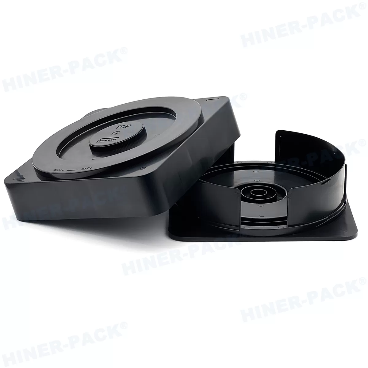
Evaluating Your Wafer Box Quotation for Long-Term Value
A thorough evaluation of a wafer box quotation goes beyond comparing unit prices. Semiconductor procurement teams should assess the total value by reviewing the manufacturer's testing protocols and quality assurance documentation.
A professional proposal should include verification of key parameters, such as Outgassing Analysis (via gas chromatography-mass spectrometry), Liquid Particle Counts (LPC), and Ion Chromatography testing to verify low ionic contamination levels. Additionally, verifying the reusability of the carrier is important; a more durable carrier with a higher initial cost can offer a lower cost per use over its operational life compared to single-use options.
Working with an experienced manufacturer like Hiner-pack ensures that all engineering specifications, cleanliness standards, and logistics details are fully documented. This level of transparency helps procurement teams make informed decisions that safeguard production yields and optimize supply chain operations.
Procurement and Engineering Cooperation
Selecting the right wafer transport system requires coordination between engineering and procurement. While procurement focuses on cost structures and lead times, packaging engineers must verify that material selections prevent chemical outgassing and electrostatic damage during transport.
To facilitate a precise evaluation, engineering teams should provide detailed operating parameters, including automated handling specifications, process chemical exposures, and target shipping distances. Sharing these parameters helps ensure the initial proposal is aligned with operational requirements, minimizing the need for subsequent design modifications.
By establishing a clear understanding of material grades, cleanroom manufacturing standards, and logistics requirements, semiconductor organizations can establish reliable supply chains. For a detailed analysis tailored to your specific wafer handling and transport requirements, please submit a formal inquiry to our technical sales team at Hiner-pack.
Frequently Asked Questions
Q1: What standard information is required to receive an accurate wafer box quotation?
A1: To provide an accurate proposal, Hiner-pack requires details on the wafer diameter (e.g., 150mm, 200mm, 300mm), wafer thickness, payload capacity (single-wafer coin shipper versus 25-capacity horizontal shipper), ESD protection requirements (conductive, dissipative, or natural polymer), and cleanroom packaging standards (double-bagged ISO class level).
Q2: How does material selection for ESD protection affect the unit pricing in a quotation?
A2: Conductive polymer compounds using carbon-filled resins represent a cost-effective choice for standard shipping needs. However, for ultra-clean semiconductor processing where carbon shedding is a concern, inherently dissipative polymers (IDP) are utilized. IDPs prevent particle shedding and offer stable surface resistivity, but carry a premium raw material cost that is reflected in the quotation.
Q3: Why are cleanroom manufacturing certifications listed on the quotation?
A3: Wafer shipping boxes must be free from microscopic particles and ionic residues to prevent wafer contamination. Manufacturing, washing, and packaging within certified cleanrooms (such as ISO Class 5 or Class 4 environments) require specialized filtration, ultrapure DI water washing, and particle monitoring. These procedures ensure compliance with semiconductor purity standards and are detailed in the proposal to verify product quality.
Q4: Does Hiner-pack support custom design options for non-standard wafer thicknesses?
A4: Yes. Standard shippers are designed for standard SEMI wafer thicknesses. For thin wafers (e.g., back-grinded or ultra-thin wafers) or thick compound semiconductor substrates (such as SiC or Sapphire), custom internal retention cushions or modified spring designs are required. These specialized requirements are quoted based on custom mold design or custom elastomeric insert fabrication.
Q5: What are the typical lead times after accepting a wafer box quotation?
A5: Lead times depend on whether the requested item is a standard off-the-shelf catalog configuration or a customized design. Standard products typically ship within 2 to 4 weeks, subject to production schedules and raw material availability. Custom configurations requiring mold modifications or custom material compounding generally require 6 to 10 weeks for tooling validation and initial production sampling.














