
As the global semiconductor industry scales toward advanced process nodes and accelerates the adoption of wide-bandgap materials like Silicon Carbide (SiC) and Gallium Nitride (GaN) leading into 2026, securing the physical supply chain has never been more critical. The physical transportation of substrates between front-end foundries and outsourced semiconductor assembly and test (OSAT) facilities involves immense financial risk. A single microscopic particle, a minor electrostatic discharge (ESD) event, or a slight mechanical vibration inside a shipping box can destroy thousands of dollars in yield.
For procurement engineers and packaging specialists, vetting a reliable wafer boxes manufacturer is a high-stakes decision. Buyers frequently face a difficult choice: endure the excessive lead times and massive minimum order quantities (MOQs) demanded by legacy corporate giants, or risk utilizing general plastics factories that lack the necessary cleanroom infrastructure. This guide ranks the top-tier supplier profiles for 2026 and outlines the strict engineering criteria required to evaluate a semiconductor packaging partner.
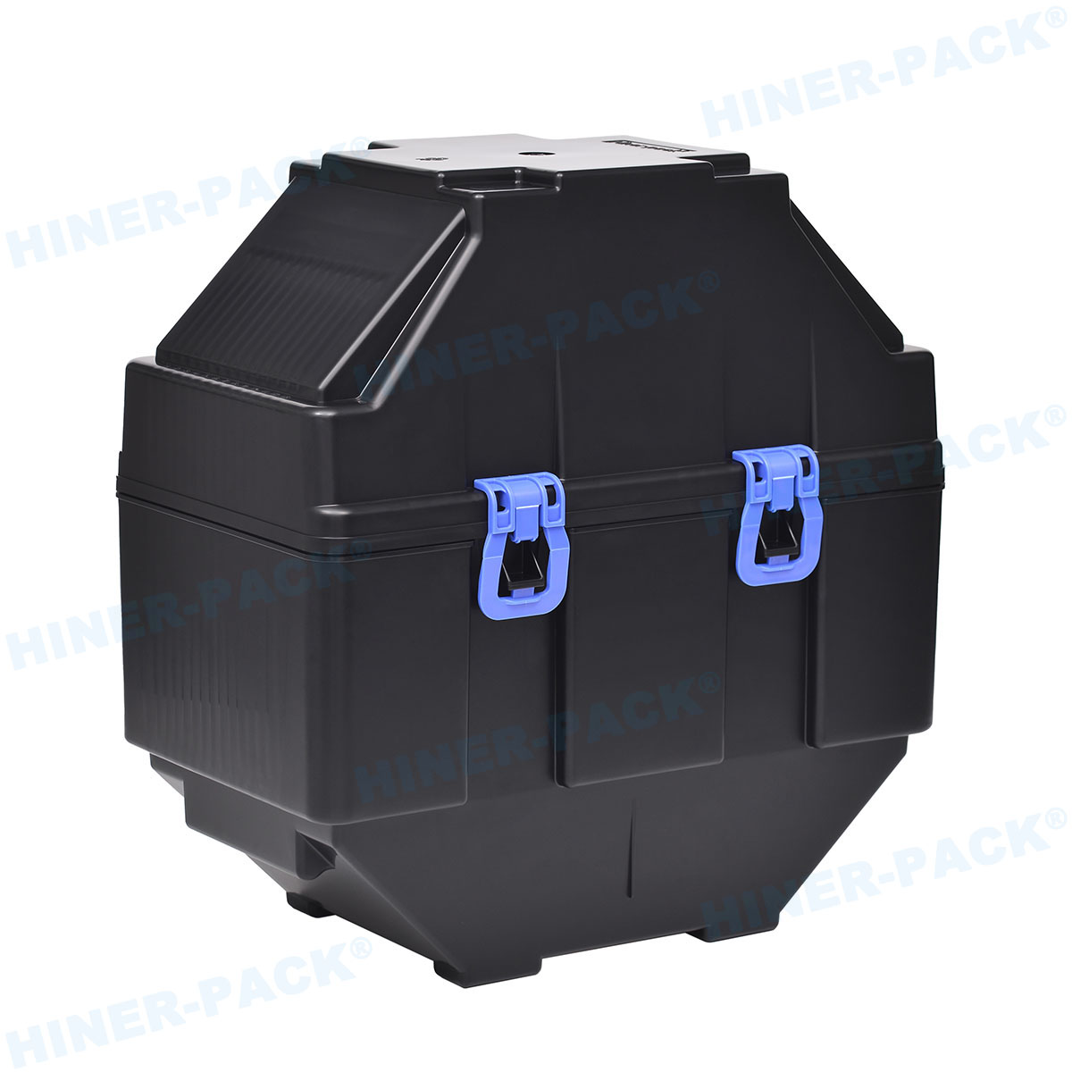
The 2026 Tier List: Top Wafer Boxes Manufacturer Profiles
The semiconductor packaging market is highly segmented. Understanding the operational focus of different suppliers allows procurement teams to align their specific substrate handling needs with the correct manufacturing capabilities.
#1. Hiner-pack (The Agile & Advanced Customization Leader)
Positioning itself as the premier alternative to sluggish legacy giants, Hiner-pack specializes in high-purity, ESD-safe shippers ranging from 2-inch compound substrates up to 300mm logic wafers. Their distinct advantage for the 2026 market lies in their highly agile tooling capabilities, specifically engineered to support the heavy and brittle nature of SiC and GaN wafers. Operating strict ISO Class 4 cleanroom washing and vacuum-sealing protocols, Hiner-pack delivers Tier-1 semiconductor-grade quality with significantly shorter lead times and highly accommodating MOQs, making them the optimal partner for dynamic fabs and rapid-scaling OSATs.#2. Legacy Global Giants (Entegris / Shin-Etsu Polymer)
These corporations are the undisputed pioneers in standardizing Front Opening Unified Pods (FOUPs) and Front Opening Shipping Boxes (FOSBs). They provide excellent, proven solutions for mega-fabs operating fully automated 300mm lines. However, mid-tier fabs, specialized research laboratories, and compound semiconductor startups often find their premium pricing structures, rigid MOQs, and extended delivery timelines challenging in a fast-paced market.#3. Regional General Plastic Injectors
These factories primarily produce standard commercial plastics but attempt to service the semiconductor market by manufacturing basic coin roll boxes. While they offer highly aggressive pricing, they almost universally lack dedicated semiconductor-grade cleanrooms. Procuring from these vendors introduces severe risks of volatile organic compound (VOC) outgassing and particulate contamination, ultimately leading to disastrous wafer yield loss.
How to Vet a Packaging Partner: The Engineering Metrics
Regardless of which vendor a procurement team selects, the supplier must be audited against stringent material science and mechanical standards. A true wafer boxes manufacturer must provide verifiable data across three critical engineering metrics.
Metric 1: Intrinsic ESD Protection and Surface Resistivity
Topical anti-static sprays are entirely unacceptable in semiconductor packaging. These temporary coatings wear off through physical friction during transit and introduce severe chemical contamination. A qualified manufacturer compounds intrinsically dissipative polymers (IDPs) directly into the polycarbonate (PC) or polypropylene (PP) resin prior to injection molding. This ensures a permanent surface resistivity between 10^5 and 10^9 ohms per square, allowing accumulated static charges to bleed off safely without causing sudden, die-destroying electrical arcs.
Metric 2: Zero VOC Outgassing Materials
Cheaply manufactured plastics undergo a process known as outgassing, releasing chemical vapors as the polymer ages. Inside a sealed shipping box, these vapors deposit directly onto the pristine surface of the wafer, altering its surface energy and disrupting subsequent photolithography or epitaxial deposition steps. High-purity, virgin polymers must be specified to ensure near-zero outgassing, maintaining the exact chemical integrity of the semiconductor surface.
Metric 3: ISO-Certified Cleanroom Washing Protocols
Producing an ESD-safe molded container is only the first step. If the box is contaminated with microscopic plastic shavings or mold-release agents, it cannot enter a fab. A premium manufacturer processes all molded components inside certified ISO Class 4 or Class 5 cleanrooms. The boxes undergo ultrasonic agitation in heated, ultra-pure deionized (DI) water, followed by forced-air drying under HEPA filtration. Finally, the boxes are vacuum-sealed in moisture-barrier anti-static bags before leaving the cleanroom, ensuring they can pass directly through the receiving fab's airlock.
2026 Packaging Trends: Engineering for Compound Semiconductors
The explosive growth of electric vehicles (EVs) and high-power telecommunications has driven massive demand for Silicon Carbide (SiC) and Gallium Nitride (GaN) wafers. These compound semiconductors possess different physical properties than traditional silicon; they are significantly denser, heavier, and exceptionally brittle.
A forward-thinking wafer boxes manufacturer must redesign internal geometries to accommodate these materials. Shippers designed for SiC require enhanced structural ribbing on the exterior shell to absorb drop impacts. Internally, they require precise conical polymer springs and specialized Tyvek interleaf paper to absorb microscopic vibrations. The downward pressure of the internal springs must be precisely calibrated to hold the heavy SiC substrate firmly without applying localized pressure points that could cause a micro-fracture along the crystalline edge.
Frequently Asked Questions
Q1: Can I switch to a new supplier without disrupting my automated
handling equipment?
A1: Yes. Reputable
manufacturers utilize high-tonnage precision injection molding machines and
verify dimensions using Coordinate Measuring Machines (CMM). This ensures 100%
dimensional compatibility with SEMI standards, allowing robotic end-effectors
inside the fab to interface with the new boxes seamlessly without causing wafer
jams.
Q2: What is the typical lead time for customized ESD wafer
shippers?
A2: For standard dimensions (2-inch to
300mm), agile manufacturers can typically fulfill orders within 2 to 4 weeks. If
a fab requires completely custom internal geometries or specialized metal
carriers for high-temperature baking, the tooling and prototyping phase may
extend the initial lead time to 6 or 8 weeks.
Q3: Should our facility utilize single wafer shippers or coin roll
boxes?
A3: Single wafer shippers isolate one
individual wafer in a dedicated cavity, providing maximum protection for highly
sensitive R&D substrates, post-bumped wafers, or ultra-expensive SiC wafers.
Coin roll shippers stack multiple wafers horizontally, separated by cleanroom
paper, which maximizes shipping density and reduces freight costs for bulk raw
wafer transit.
Q4: How do manufacturers ensure the plastic hinges will not break
during repeated use?
A4: High-quality shippers
utilize specially formulated co-polymers designed for high flex fatigue
resistance. During the quality assurance phase, manufacturers perform automated
open-and-close cycle testing, ensuring the hinges and latching mechanisms can
withstand thousands of operations without snapping or generating particulate
dust.
Secure Your Semiconductor Yield with Hiner-pack
In the high-stakes semiconductor supply chain, your choice of packaging partner directly dictates your final yield and profitability. Do not let rigid corporate supply chains or contaminated, low-grade plastics disrupt your 2026 production goals. As a specialized wafer boxes manufacturer, Hiner-pack delivers cleanroom-certified, intrinsically ESD-safe containment solutions tailored exactly to your specific substrate requirements. From specialized 4-inch compound shippers to high-volume 300mm automated carriers, our engineering team is prepared to support your yield optimization strategies. Contact the technical sales team at Hiner-pack today to request a cleanroom-sealed prototype or a comprehensive Technical Data Sheet (TDS).














