
In the global semiconductor supply chain, the physical transit of silicon and compound substrates between front-end foundries and outsourced assembly and test (OSAT) facilities represents a period of extreme vulnerability. When procurement directors and fab managers evaluate the wafer boxes price, they must contextualize this expense against the astronomical value of the cargo being transported. A single fully processed 300mm logic wafer can hold hundreds of thousands of dollars in commercial value. Consequently, purchasing semiconductor packaging based solely on the lowest initial unit cost is a flawed procurement strategy. Evaluating shipping containers requires analyzing the total cost of ownership (TCO), understanding the complex manufacturing infrastructure that dictates the price, and recognizing that premium packaging serves as a critical insurance policy against catastrophic yield loss.
Deconstructing the Cost: Material Science and ESD Protection
The baseline driver of the wafer boxes price is the chemical engineering required to synthesize the base polymer. Commercial-grade plastics act as electrical insulators, accumulating massive static charges through friction during transit. A sudden discharge into a delicate semiconductor circuit will instantly rupture the gate oxide layer, rendering the die useless.
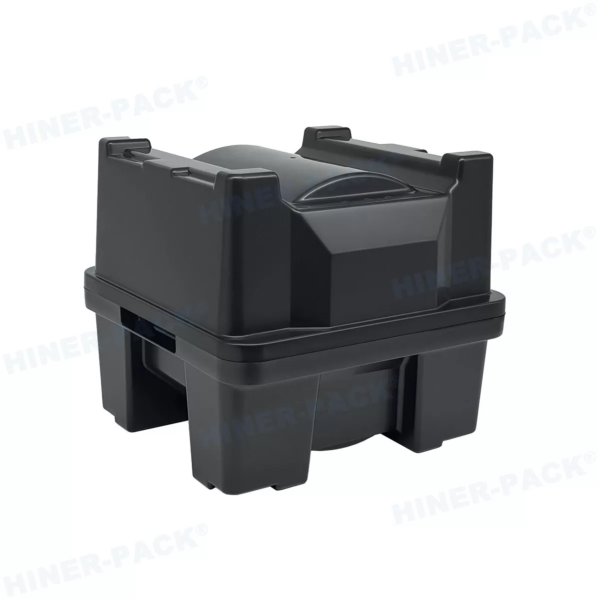
To mitigate this, high-end packaging manufacturers utilize advanced polymers, such as carbon-loaded polycarbonate (PC) or engineered polypropylene (PP). These materials are intrinsically static-dissipative, offering a consistent surface resistivity between 10^5 and 10^9 ohms per square. Synthesizing these high-purity, zero-outgassing resins requires significant thermal and chemical control, establishing a higher baseline cost than standard industrial plastics. Procurement teams must understand that paying a premium for these specific material properties directly prevents uncorrectable electrostatic discharge (ESD) damage upon opening the box in the receiving cleanroom.
The Hidden Value: Cleanroom Processing Infrastructure
A significant portion of the wafer boxes price reflects the environmental controls necessary to prepare the container for immediate fab entry. An injection-molded box is inherently contaminated with microscopic plastic dust and trace mold-release agents. If a manufacturer ships these unwashed boxes, the buyer assumes the massive financial burden of decontaminating the packaging onsite.
Premium suppliers operate dedicated ISO Class 4 or Class 5 cleanroom environments. Inside these sterile facilities, the newly molded boxes undergo rigorous ultrasonic agitation in heated, 18-megohm Deionized (DI) water. The components are then dried under HEPA filtration and immediately vacuum-sealed within moisture-barrier, anti-static bags. While this intensive, multi-stage decontamination process increases the initial procurement quotation, it saves the purchasing facility immense operational expenditures (OPEX) by allowing the sealed boxes to pass directly through the material airlock without requiring secondary washing protocols.
Pricing Variations Based on Form Factor and Geometry
The specific architecture of the container dictates the volume of raw material used and the complexity of the injection mold tooling, directly influencing the final unit price.
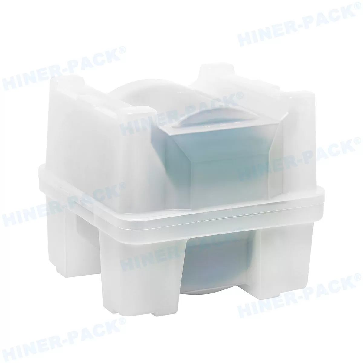
Single Wafer Shippers: Designed for highly sensitive post-bumped wafers or extremely brittle compound substrates like Silicon Carbide (SiC) and Gallium Nitride (GaN). These units require precise internal conical springs to immobilize the substrate. Because they house only one wafer, the cost-per-wafer ratio is higher, but the isolation provides maximum mechanical protection for high-value R&D or specialty lots.
Coin Roll Shippers: The most economical format for transporting bulk volumes of raw, unprocessed silicon or dummy wafers. Wafers are stacked horizontally and separated by cleanroom-grade Tyvek interleaf paper. The simplistic, high-capacity design of the container drastically lowers the packaging cost per wafer.
Multi-Slot Cassettes and FOSBs: Front Opening Shipping Boxes (FOSB) designed for automated 300mm lines represent the peak of packaging complexity. They require massive, high-tonnage injection molding presses to ensure zero dimensional warping. Because robotic end-effectors rely on microscopic dimensional tolerances to extract wafers without jamming, these units command the highest price point within the packaging hierarchy.
Frequently Asked Questions
Q1: How do volume discounts affect the overall wafer boxes
price?
A1: As with most injection-molded components, unit economics
improve dramatically with scale. Operating the high-temperature molds and
maintaining cleanroom washing lines carry high fixed setup costs. Procurement
teams ordering full container loads (FCL) will secure significantly lower
per-unit pricing compared to buyers placing minimal quantity pilot orders.
Q2: Does customizing the internal springs for thicker wafers increase
the cost?
A2: If the manufacturer must CNC machine entirely new
steel mold inserts to accommodate non-standard wafer thicknesses, an initial
tooling fee (NRE) will be applied. However, once the mold is established, the
ongoing per-unit production cost remains comparable to standard items.
Q3: Are there pricing differences between clear and opaque black
shippers?
A3: Opaque black or dark blue shippers heavily loaded with
conductive carbon black often carry slightly different pricing than translucent
static-dissipative polymers. The choice should be driven by whether the specific
semiconductor material is highly sensitive to ultraviolet (UV) light degradation
during transit.
Q4: Is it more cost-effective to wash packaging in-house or buy
pre-washed cleanroom boxes?
A4: Purchasing pre-washed, vacuum-sealed
boxes is vastly more cost-effective for the majority of fabs and OSATs.
Operating an internal DI water ultrasonic line requires heavy capital
investment, continuous energy consumption, and significant wastewater treatment
logistics.
Q5: Why do shippers for Silicon Carbide (SiC) sometimes cost more
than those for standard silicon?
A5: SiC substrates are
significantly denser and heavier than standard silicon. Shippers designed for
these compound materials require reinforced external ribbing and higher-tension
internal polymer springs to absorb kinetic impact and prevent edge chipping,
utilizing more raw material in the manufacturing process.
Secure Competitive Sourcing with Hiner-pack
Protecting your semiconductor yield requires partnering with a manufacturer who views packaging as a critical engineering discipline, rather than a commodity plastic transaction. At Hiner-pack, we bridge the gap between uncompromising quality and aggressive supply chain economics. By operating our own high-tonnage injection presses, ISO-certified cleanroom washing lines, and internal metrology laboratories, we eliminate intermediary trading markups. This direct-to-manufacturer relationship ensures our B2B partners receive a highly transparent, competitive wafer boxes price without sacrificing ESD safety or outgassing standards. Whether your facility requires agile tooling for emerging SiC substrates or massive volumes of standard coin roll shippers, our engineering sales team is prepared to optimize your procurement budget. Contact Hiner-pack today to request an official wholesale quotation and arrange for cleanroom-certified testing samples.














