
Procuring specialized packaging for semiconductor manufacturing is a high-stakes financial operation. When supply chain managers and fab engineers request a wafer boxes quotation, they are attempting to secure containment solutions for cargo that can hold hundreds of thousands of dollars in commercial value. In this sector, accepting a supplier's proposal based solely on the lowest bottom-line figure is a severe operational risk. A dramatically underpriced quote often indicates dangerous shortcuts in polymer science or cleanroom processing. To protect both the fabrication yield and the operational budget, procurement teams must understand exactly how a professional manufacturer calculates their pricing. This guide deconstructs the specific engineering and processing variables that dictate an accurate, comprehensive pricing proposal.
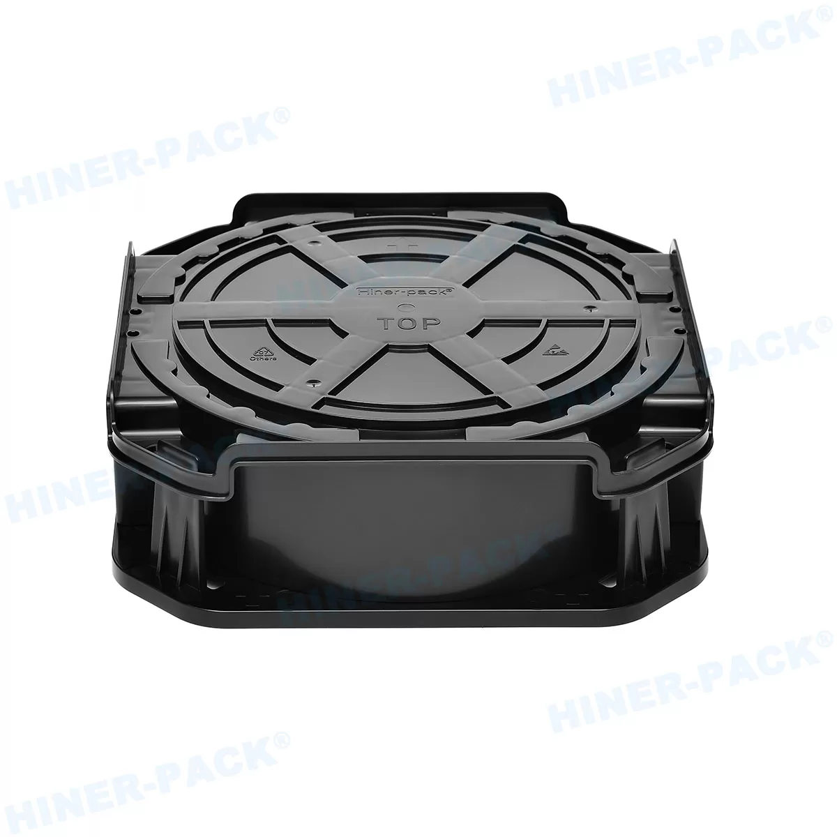
Deconstructing the RFQ: NRE Tooling vs. Unit Costs
When reviewing a commercial proposal from a manufacturing partner, the pricing structure is typically divided into distinct categories. Understanding the separation between capital tooling expenses and recurring unit costs prevents budget overruns.
For custom packaging geometries, the quotation will list Non-Recurring Engineering (NRE) charges. This fee covers the CAD design, CNC machining, and polishing of the heavy steel injection molds required to form the plastic shells and internal retaining springs. NRE is a one-time capital expenditure. If a fab requires a completely bespoke shipper designed to hold an irregular substrate, the NRE cost will reflect the complexity of that specific steel mold.
The unit cost represents the price per individual box produced. This figure operates on a sliding scale based on the Minimum Order Quantity (MOQ). Injection molding machines carry high thermal setup and changeover costs. A wafer boxes quotation for a massive 10,000-unit production run will demonstrate a significantly lower per-unit cost than a small 500-unit pilot batch, as the factory's setup overhead is amortized across a much larger volume of plastic.
Material Science: The Price of True ESD Protection
The chemical formulation of the plastic substrate fundamentally drives the raw material cost. Standard commercial plastics are highly insulative and generate massive static charges during transit. A sudden static discharge into a delicate silicon circuit destroys the gate oxide layer instantly.
A legitimate proposal for semiconductor packaging will specify the use of intrinsic static-dissipative polymers, such as engineered polycarbonate (PC) or carbon-loaded polypropylene (PP). These high-purity resins are chemically synthesized to maintain a permanent surface resistivity between 10^5 and 10^9 ohms per square. Because these advanced polymers require strict compounding controls to prevent volatile outgassing and particle shedding, their raw material cost is inherently higher than standard plastics. If a competing quote is suspiciously cheap, the supplier may be utilizing standard plastics coated with temporary anti-static sprays, a highly contaminating practice that is entirely unacceptable inside a cleanroom environment.
Cleanroom Processing and Decontamination Fees
A bare injection-molded plastic box is covered in microscopic polymer dust and mold-release agents. The most critical component of a comprehensive wafer boxes quotation is the inclusion of professional decontamination protocols.
Premium manufacturers operate dedicated wet-processing lines inside certified ISO Class 4 or Class 5 cleanrooms. The pricing reflects the intensive labor and energy required to submerge the components in heated, ultrasonic tanks filled with ultra-pure Deionized (DI) water. Following the ultrasonic scrub, the components are dried under HEPA filtration and immediately vacuum-sealed inside moisture-barrier anti-static bags. A quotation that omits these cleanroom washing and vacuum-sealing steps forces the purchasing fab to absorb the massive financial and logistical burden of decontaminating the raw boxes onsite before they can enter the production airlock.
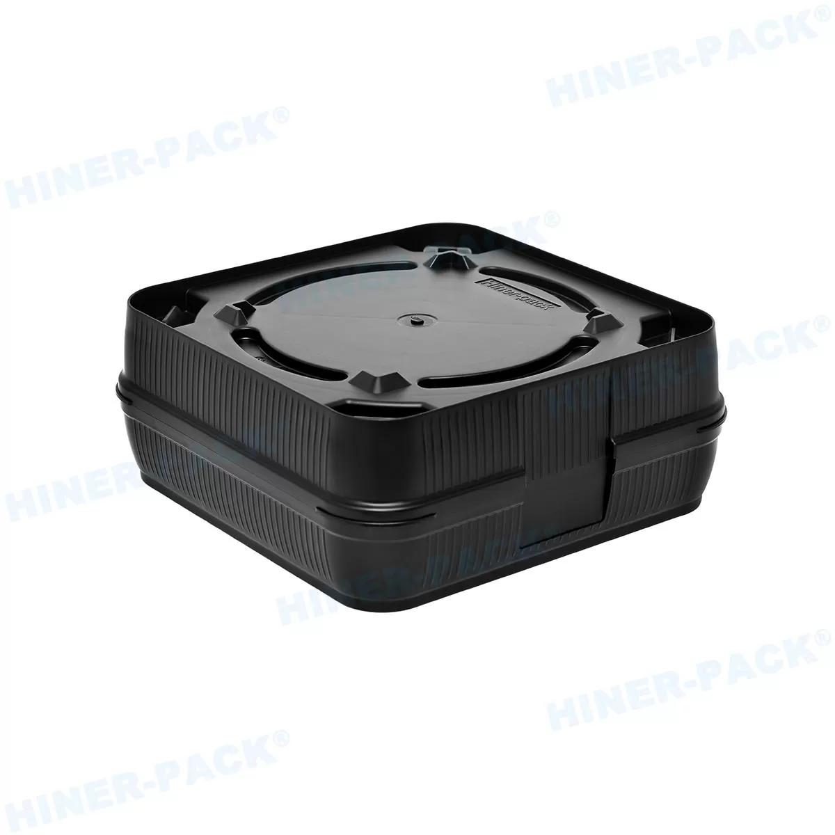
Substrate Specifications: Silicon vs. Compound Materials
The physical properties of the specific wafer being transported directly influence the internal engineering of the box, which in turn alters the manufacturing cost.
Standard silicon wafers require specific downward pressure from the internal conical springs to prevent vibration. However, the rapidly expanding market for compound semiconductors, such as Silicon Carbide (SiC) and Gallium Nitride (GaN), has introduced new packaging requirements. SiC substrates are significantly denser, heavier, and more brittle than standard silicon. A quotation for SiC shippers will reflect the necessity of thicker external ribbing for impact resistance and highly calibrated polymer springs designed to immobilize the heavy substrate without creating localized pressure points that could cause edge fractures.
Frequently Asked Questions
Q1: What specific details should I provide to receive an accurate
quotation?
A1: To generate a precise quote, suppliers require the exact wafer
diameter, the wafer thickness (especially if dealing with thinned or back-ground
wafers), the required material (PC, PP, or PFA for chemical resistance), target
order volumes, and whether the application requires single shippers, coin roll
boxes, or multi-slot cassettes.
Q2: Does the quotation typically include international shipping
logistics?
A2: Most initial manufacturing quotes are provided on an EXW (Ex
Works) or FOB (Free On Board) basis, covering only the manufacturing and
domestic port delivery. Buyers should explicitly request CIF (Cost, Insurance,
and Freight) or DDP (Delivered Duty Paid) terms if they require the manufacturer
to manage the entire international ocean or air freight logistics chain.
Q3: Are tooling (NRE) costs refundable if I place a massive bulk
order?
A3: Many professional manufacturers offer tooling amortization
agreements. Under these terms, if the buyer commits to and successfully orders a
predetermined high volume of units over a specific contractual period, the
factory will rebate the initial NRE tooling fee.
Q4: Why is the price for clear shippers sometimes different from opaque black
shippers?
A4: Opaque black shippers are heavily loaded with conductive carbon
black, which alters the resin cost and provides excellent protection for
UV-sensitive substrates. Clear, translucent shippers require different
dissipative chemical additives to maintain optical clarity while preserving ESD
safety, resulting in slight variations in raw material pricing.
Q5: Can I request physical samples before approving a bulk quotation?
A5:
Yes. Reputable manufacturers always encourage physical sample validation. Buyers
can request a small batch of cleanroom-sealed prototypes to conduct internal
drop tests, verify robotic handling compatibility, and perform surface
resistivity checks before signing the final mass production contract.
Optimize Your Procurement Strategy with Hiner-pack
Protecting your semiconductor yield requires partnering with a facility that treats packaging manufacturing with the same rigorous discipline as a semiconductor foundry. Relying on opaque pricing or substandard materials introduces catastrophic risks to your supply chain.
At Hiner-pack, we bridge the gap between uncompromising cleanroom quality and aggressive supply chain economics. Operating as a fully integrated factory, we control the entire process from precision injection molding and ISO-certified DI water washing to final vacuum sealing. By bypassing trading intermediaries, we provide our B2B partners with highly transparent pricing structures devoid of hidden decontamination or handling fees. Whether your facility requires agile tooling for emerging compound substrates or high-volume automated cassettes, our engineering teams are prepared to optimize your procurement budget.
Contact the commercial sales division at Hiner-pack today to submit your RFQ, request physical cleanroom samples, and secure a comprehensive wafer boxes quotation tailored to your exact floor requirements.














