
Semiconductor manufacturing demands extreme precision. A single speck of dust or an unexpected electrostatic discharge can ruin millions of dollars in delicate silicon wafers. During fabrication, dicing, and final assembly, these components travel between machines, facilities, and continents. Protecting them requires specialized handling equipment.
Choosing the right wafer tray factory is a strategic decision that directly affects your production yield. Poorly manufactured carriers introduce particulate contamination, static damage, and mechanical stress. Modern semiconductor facilities need a manufacturing partner that understands cleanroom environments and material science.
Founded in 2013, Hiner-pack® has established itself as a comprehensive, one-stop supplier for automated handling, carrying, and transport solutions. As a dedicated wafer tray factory, Hiner-pack® delivers cleanroom-grade protection engineered to keep your microchips safe across every stage of production.
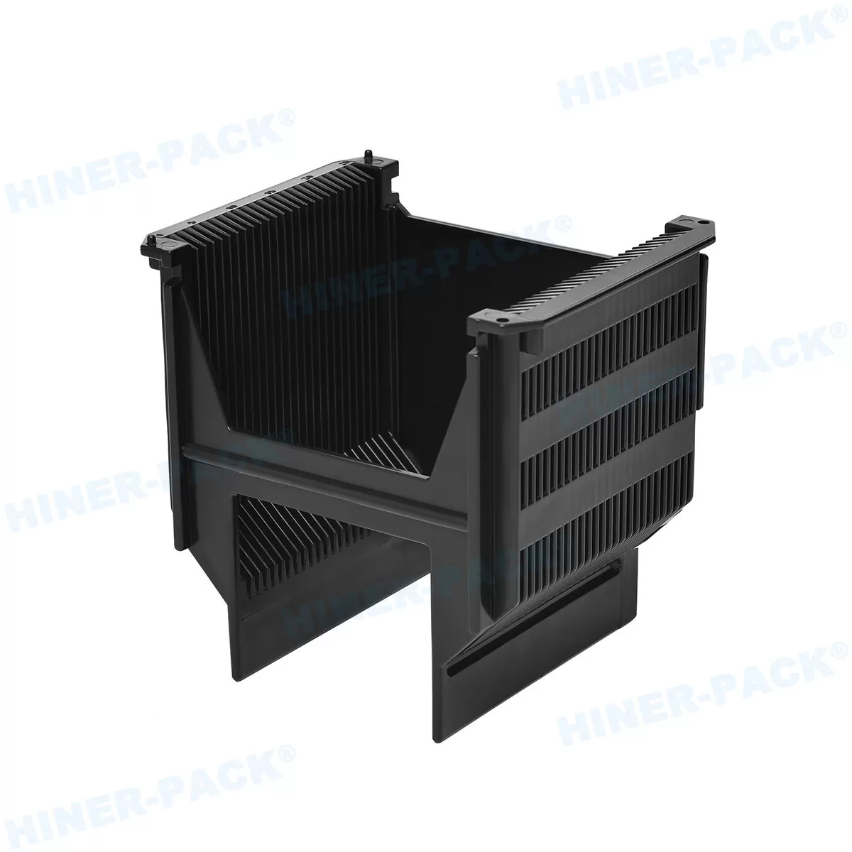
Why Partner with a Dedicated Wafer Tray Factory?
Off-the-shelf plastic containers cannot meet the strict demands of modern semiconductor packaging. Advanced integrated circuits require specialized designs, ultra-clean production setups, and exact static dissipation parameters. Partnering directly with a qualified wafer tray factory gives you total control over cleanroom compliance, custom molds, and raw material selection.
Cleanroom Precision Manufacturing
Contamination control remains the top priority for semiconductor packaging. A high-standard wafer tray factory must operate controlled cleanroom environments to prevent air particulates from landing on plastic carriers during molding and washing.
Hiner-pack® maintains strict cleanroom standards throughout our manufacturing processes:
Controlled Injection Molding: Our automated injection molding machines operate inside high-grade cleanrooms to prevent ambient particle contamination during forming.
Ultra-Clean Ultrasonic Washing: Every carrier passes through automated multi-stage ultrasonic cleaning lines using deionized (DI) water to clear microscopic debris.
Low Particulate Count: We test finished products under optical particle counters to ensure they meet stringent international cleanroom wafer packaging standards.
Vacuum Cleanroom Packaging: Products are double-bagged inside cleanroom environments to guarantee they arrive at your facility in pristine condition.
Advanced Material Science and Static Control
Static electricity is a silent killer in microelectronics. Electrostatic discharge (ESD) can melt internal chip interconnects without leaving any visible exterior marks. A professional wafer tray factory must formulate precise polymers that drain static charges safely.
In collaboration with leading university polymer research institutes, Hiner-pack® develops high-performance material blends tailored for sensitive electronics:
ESD Safe Wafer Trays: We control surface resistivity precisely within the electro-conductive or static-dissipative range ($10^4$ to $10^{11}$ ohms/sq).
Low Outgassing Polymers: Our raw materials release minimal volatile organic compounds (VOCs), preventing chemical fogging on delicate wafer surfaces.
High Thermal Resistance: We process advanced engineering plastics like Polycarbonate (PC), Polypropylene (PP), PEEK, and PES to withstand high-temperature processing and chemical exposures.
Precision Injection Molding and Tooling
Silicon wafers are exceptionally thin and fragile. Carrier dimensions must match automated pick-and-place machinery with sub-millimeter tolerances. Warped pocket walls or imprecise pocket depths cause machine jams, mechanical chipping, and costly production downtime.
As a full-service wafer tray factory, Hiner-pack® operates an in-house precision mold tooling center. We manufacture standardized and custom carrier formats ranging from 2-inch, 3-inch, 4-inch, 6-inch, and 8-inch up to 12-inch wafer sizes. Whether you need a simple coin box, a pocketed wafer tray, or a heavy-duty frame shipper, our precision molds maintain strict dimensional consistency across millions of units.
Comprehensive Semiconductor Carrier Solutions
Different steps in the semiconductor supply chain demand different packaging configurations. A modern wafer tray factory must offer a versatile product lineup to support bare die handling, sliced wafer transport, and automated IC testing.
Hiner-pack® provides an extensive range of semiconductor carrier solutions built for safety and ease of automation integration.
Wafer Trays and Wafer Shippers
Our standard wafer trays and shippers protect bare wafers, ultra-thin wafers, and diced chips during inter-factory transit. We engineer every pocket with smooth, non-abrasive contact surfaces to prevent edge chipping or surface scratching.
Single Wafer Shippers (Coin Boxes): Ideal for safe, secure transport of individual research wafers, substrates, or high-value optical components.
Multi-Pocket Wafer Trays: Designed for high-density storage and manual or automated transfer of loose die and delicate substrates.
Vacuum Release Trays: Feature specialized gel surfaces or mesh bottom profiles to hold delicate bare die securely during transit without edge contact.
Frame Shippers for Dicing and Tape Processes
After wafer dicing, silicon chips sit mounted on flexible adhesive tape held by rigid metal or plastic frames. Transporting these expanded film frames requires specialized outer shipping boxes.
Hiner-pack® builds rugged, highly stable frame shippers that hold dicing frames securely in place. These carriers feature ESD-safe materials and rigid structural ribs to prevent internal flexing, keeping dicing tape taut and preventing die-to-die collisions during global freight transport.
JEDEC Standard Matrix Trays and Process Carriers
Automated packaging and testing lines require standard dimensions to ensure smooth robot loading. Hiner-pack® produces a wide range of JEDEC-standard matrix trays designed for automated pick-and-place equipment.
High-Temperature Bakeable Trays: Manufactured from special heat-resistant compounds to endure high-temperature chip baking and testing cycles without warping.
Non-Bakeable Transport Trays: Cost-effective, ESD-safe options for shipping finished IC packages between assembly and testing sites.
Process Cassettes: Precision-molded carriers designed for smooth transfer through automated chemical, cleaning, and inspection machinery.
Technical R&D and Quality Control
Manufacturing semiconductor packaging is an exact science. Maintaining leadership as an international wafer tray factory requires continuous investment in research, equipment, and certified quality management systems.
Hiner-pack® operates as an innovation hub that drives domestic and international advancements in semiconductor transport carriers. Our facility holds multiple utility and design patents covering non-marking pocket designs, static dissipation methods, and shock-resistant outer shell structures.
Rigorous Quality Inspection System
We do not rely on spot checks. Hiner-pack® enforces strict quality control steps throughout the entire production lifecycle:
Dimensional Accuracy Testing: Coordinate Measuring Machines (CMM) verify that pocket dimensions, wall flatness, and outer stack features match technical drawings exactly.
Surface Resistivity Testing: Resistance meters test every production batch at multiple surface points to confirm consistent ESD protection.
Cleanroom Particulate Audits: Finished lots undergo liquid particle counting and optical surface inspection before leaving the cleanroom packaging area.
Chemical Outgassing Analysis: We monitor material formulations to guarantee low outgassing levels, protecting sensitive optical coatings and metallic pads from degradation.
Custom Wafer Shipper Design and Engineering
Standard off-the-shelf carriers do not fit every custom chip geometry or automated line. When standard shapes fall short, our dedicated engineering team creates specialized custom wafer shipper designs tailored to your exact process specifications.
We analyze your target substrate thickness, automated gripper tolerances, static requirements, and shipping environments. Using 3D prototyping and mold flow analysis, Hiner-pack® turns custom concepts into tested, high-volume production molds in industry-leading lead times.
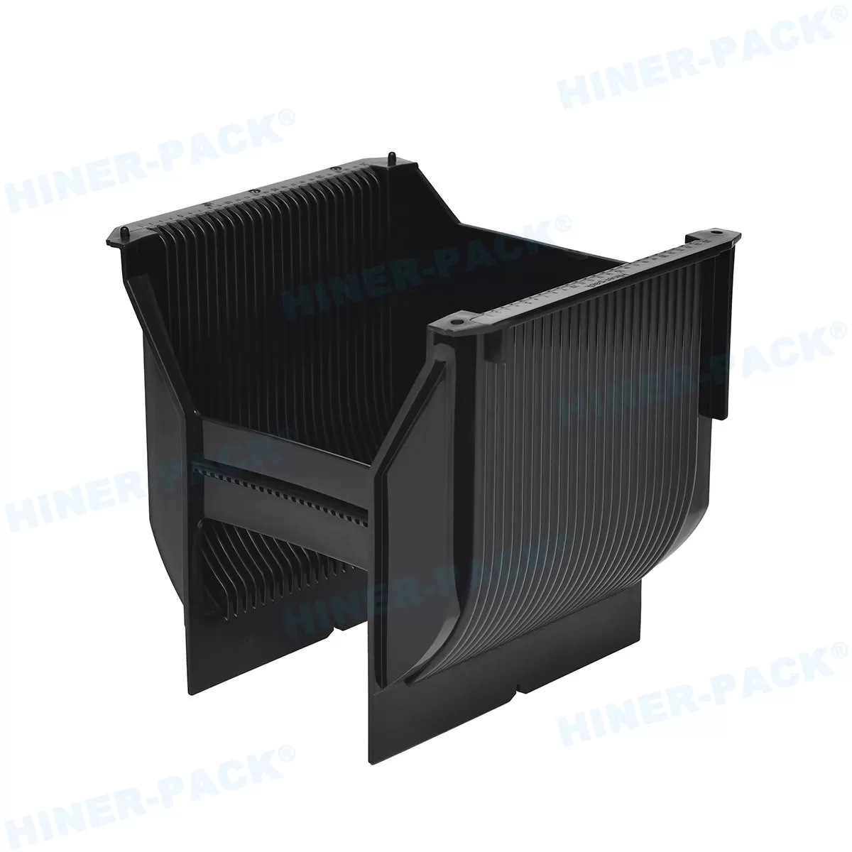
Secure Your Semiconductor Supply Chain Today
Your microchips represent huge investments of time, energy, and engineering talent. Do not let low-quality packaging compromise your final yield. Partnering with a proven, technology-driven wafer tray factory gives your products the physical protection and cleanroom purity they require.
Hiner-pack® brings over a decade of manufacturing experience, advanced material R&D, and cleanroom production capabilities to your supply chain. We are more than a production facility—we are your strategic technical partner for complete semiconductor handling and shipping safety.
Are you ready to improve your packaging reliability and protect your yield rates? Contact the technical sales team at Hiner-pack® today. Request free product samples, discuss custom wafer shipper tooling, or schedule a formal factory audit of our cleanroom facilities.
Frequently Asked Questions (FAQ)
Q1: What cleanroom standards does Hiner-pack® maintain for wafer tray
manufacturing?
A1: Hiner-pack® operates cleanroom
injection molding and multi-stage ultrasonic cleaning facilities. Products are
washed in high-purity DI water systems and packaged inside controlled cleanrooms
to guarantee minimal particulate contamination and low trace-element residue on
finished trays.
Q2: Can Hiner-pack® manufacture a custom wafer shipper for
non-standard substrate sizes?
A2: Yes. As an
end-to-end wafer tray factory, we operate an in-house tooling
and engineering shop. We design and mold custom wafer shippers, unique pocket
configurations, and specialized process carriers tailored to your exact
substrate dimensions, thickness, and automation handling requirements.
Q3: How does Hiner-pack® ensure consistent ESD safety across all
wafer trays?
A3: We blend high-grade conductive and
static-dissipative additives directly into our raw engineering polymers. Every
production lot undergoes strict surface resistivity testing ($10^4$ to $10^{11}$
ohms/sq) using calibrated surface resistance meters to prevent static
accumulation and sudden electrostatic discharges.
Q4: What raw materials are used in your ESD safe wafer
trays?
A4: We work with a wide range of specialized
polymers based on your application needs, including Conductive Polycarbonate
(PC), Polypropylene (PP), PEEK, PES, and specialized low-outgassing transparent
resins for visual inspection during transport.
Q5: How can B2B buyers request sample testing or a factory audit with
Hiner-pack®?
A5: B2B clients can contact our sales
engineering department directly through our online inquiry form or email. We
provide standard product samples for engineering evaluation, ESD testing, and
automated line fitting. We also welcome on-site or virtual cleanroom factory
audits for qualification.














