
In semiconductor fabrication, packaging, and testing (FAB & OSAT), safe component transport is non-negotiable. A single electrostatic discharge (ESD) event, micro-particle contamination, or mechanical shock can ruin high-value dies. This leads to massive financial losses and delayed production schedules.
Standard JEDEC chip trays serve many basic applications well. However, modern chip designs continue to push physical, thermal, and mechanical limits. As a specialized wafer tray manufacturer, Hiner-pack frequently helps engineers evaluate whether standard off-the-shelf carriers meet their yield goals or if a tailored matrix tray design is necessary.
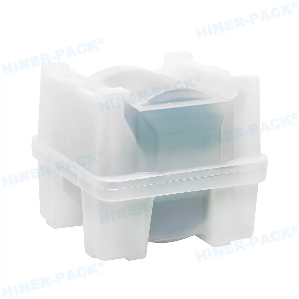
Standard Wafer Trays: Benefits & Limitations
Off-the-shelf JEDEC standard chip tray solutions are widely used across the electronics industry. They provide a quick, accessible option for standard integrated circuit (IC) footprints. Knowing when to use them—and when to walk away—is critical for protecting your yield rate.
The Benefits of Standard Trays
Lower Upfront Costs: Standard trays require no new mold tooling fees because manufacturers already possess the tooling inserts.
Fast Availability: Off-the-shelf inventory allows procurement teams to secure packaging supplies with short lead times.
Universal Industry Compatibility: Dimensions strictly follow JEDEC outline standards, fitting basic manual and automated processing equipment.
The Limitations of Standard Trays
Dimensional Mismatches: Standard pockets rarely fit non-standard die geometries, leading to excessive component movement or edge chipping during transport.
Inadequate Mechanical Protection: Ultra-thin wafers, fragile MEMS structures, or heavy power devices require targeted pocket support that stock trays cannot provide.
Generic Material Specifications: Standard stock carriers typically use baseline antistatic or conductive plastics. They often lack low-outgassing properties or high-temperature stability required for rigorous baking cycles.
Key Tipping Points: When You NEED a Custom Wafer Tray Manufacturer
While standard carriers handle mature IC packages like traditional QFN or BGA devices, specialized applications demand tailored solutions. Below are four critical scenarios where partnering with a custom wafer tray manufacturer becomes essential.
Scenario 1: Advanced Packaging & Non-Standard Dies
Modern semiconductor designs rely heavily on advanced custom semiconductor packaging techniques. Technologies like 2.5D/3D integration, Chiplets, MEMS sensors, and wide-bandgap semiconductors such as Silicon Carbide (SiC) and Gallium Nitride (GaN) feature unique aspect ratios and delicate surface structures.
Standard pocket shapes apply uneven pressure on fragile wire bonds, micro-bumps, or delicate sensor diaphragms. Using a generic tray for these components risks physical fracture or surface abrasion.
Hiner-pack addresses this challenge through precision mold design and custom tooling. By analyzing your CAD data, Hiner-pack engineers design exact pocket geometries with custom relief channels. This holds your dies securely at the perimeter, preventing direct contact with sensitive active areas and preserving component integrity.
Scenario 2: High-Speed Automated Handling & Pick-and-Place Systems
High-speed automated pick-and-place equipment relies on extreme precision. If a carrier exhibits warpage, uneven pocket depths, or broad dimensional tolerances, automated vacuum nozzles can misfeed, drop, or scratch components.
Standard trays manufactured under loose quality standards often suffer from subtle dimensional variations. These variations cause machine downtime, nozzle recalibration delays, and costly die damage during high-speed transfer.
A specialized custom wafer tray solution focuses heavily on tight tolerance control and carrier flatness. Hiner-pack integrates your equipment specifications into the tray design phase. We control critical parameters like pocket pitch, tray warp, and pocket depth tolerances down to strict limits. This ensures seamless alignment with your automated pickup tools.
Scenario 3: Specialized ESD Protection & Polymer Engineering
Static discharge remains a silent killer in microelectronics handling. Extremely sensitive devices require an ESD safe wafer carrier that maintains a tight surface resistivity window, typically between 104 and 109 Ω/sq.
Furthermore, standard ESD trays often rely on surface coatings or lower-grade antistatic additives that can slough off conductive particles or degrade over time. In high-temperature baking or cleanroom vacuum processes, inferior plastics outgas organic compounds, contaminating delicate die surfaces.
Hiner-pack overcomes these material limitations through advanced polymer modification. In partnership with top materials research institutes, Hiner-pack develops proprietary plastic compounds. We blend high-performance resins—such as MPPO, PES, or PEEK—with precise carbon fiber or carbon powder loads. This delivers permanent ESD protection, exceptional thermal resistance, and near-zero outgassing.
Scenario 4: High Cleanroom Standards & High-Value Automotive/Medical Chips
Automotive-grade (AEC-Q100) microcontrollers, medical implants, and high-power optoelectronics demand rigorous cleanliness. Microscopic airborne particles inside a carrier pocket can cause short circuits or premature field failures.
Standard off-the-shelf trays are often molded, stored, and packed in ambient factory conditions. They carry microscopic dust, residual mold release agents, and human contaminants that compromise cleanroom standards.
As a quality-focused wafer tray manufacturer, Hiner-pack operates integrated high-standard cleanroom washing lines. We process custom carriers through multi-stage ultrasonic cleaning using deionized water. Trays are dried, inspected, and double-vacuum sealed inside controlled ISO Class 5/6 cleanrooms, delivering pure, particle-free carriers directly to your production line.
Why Partner with Hiner-pack Semiconductor Solutions?
Selecting the right carrier vendor impacts your final device yield and supply chain stability. Hiner-pack provides comprehensive Hiner-pack semiconductor solutions designed to solve complex backend packaging and transport challenges.
End-to-End In-House Manufacturing
Hiner-pack manages the entire product lifecycle internally. We handle raw material formulation, mold design and machining, precision injection molding, cleanroom washing, and quality inspection under one roof. By eliminating third-party sub-contractors, we maintain total quality control and protect your proprietary designs.
Advanced R&D and Patent Portfolio
Our engineering team holds numerous patents covering carrier structural design, anti-warpage profiles, and specialized ESD material blends. We continuously innovate to meet the demands of sub-nanometer processing and advanced heterogenous integration.
Proven Track Record with Global Leaders
Hiner-pack serves leading semiconductor foundries, OSAT facilities, and fabless design firms across the globe. Our experienced application engineers understand international semiconductor quality standards and provide fast, clear design feedback.
Frequently Asked Questions (FAQ)
Q1: What is the main difference between a JEDEC standard tray and a
custom wafer tray?
A1: JEDEC standard trays follow
standardized outer dimensions and pocket grids intended for common chip sizes. A
custom wafer tray features tailored pocket geometry, precise mechanical
tolerances, and specific ESD material formulations engineered specifically for
non-standard chip shapes, ultra-thin dies, or proprietary pick-and-place
equipment.
Q2: How does a custom wafer tray manufacturer prevent damage to
ultra-thin or fragile dies?
A2: A custom wafer tray
manufacturer designs specialized pocket relief zones, soft-touch retention
features, and custom pocket depths. This minimizes physical contact with active
die surfaces while preventing lateral movement during transportation and
automated handling.
Q3: What surface resistivity ranges can Hiner-pack provide for custom
ESD trays?
A3: Hiner-pack offers customized ESD
materials with surface resistivity ranging from static dissipative
(106 to 109 Ω/sq) to fully conductive (104 to
105 Ω/sq). Our compounds ensure stable, non-degrading ESD protection
without particle migration.
Q4: What lead times should we expect when ordering custom matrix
trays from Hiner-pack?
A4: Design concept proposals
and 3D models typically take 2 to 4 business days. Prototype mold tooling and
initial physical samples are generally completed within 2 to 3 weeks. Full mass
production begins immediately after sample approval.
Q5: Can Hiner-pack process custom trays for cleanroom
environments?
A5: Yes. Hiner-pack operates
high-standard cleanroom washing lines. Custom trays undergo ultrasonic DI water
cleaning, particle inspection, and double-vacuum packaging inside ISO Class 5/6
cleanrooms to ensure immediate cleanroom readiness.
Safeguard Your Yield with the Right Carrier Partner
Choosing between standard and custom carriers comes down to component value, physical geometry, and process automation requirements. While stock JEDEC trays offer a cheap solution for standard ICs, high-value chips, advanced packaging, and automated handling demand precision engineering.
Investing in a custom matrix tray design eliminates yield losses caused by mechanical shock, static damage, particle contamination, and pick-and-place misfeeds. Partnering with an experienced wafer tray manufacturer like Hiner-pack ensures your sensitive microelectronics arrive intact at every step of the supply chain.
Ready to optimize your component transport and boost backend yields? Contact the engineering team at Hiner-pack today to discuss your project specifications, request a custom design evaluation, or order sample trays for your testing environment.














