
Semiconductor manufacturing demands extreme precision at every step. Wafers represent significant financial investment and technical effort. Yet, these fragile silicon substrates face constant threats during production, testing, and transportation.
Static electricity can instantly destroy delicate integrated circuits. Microscopic airborne contaminants degrade functional yields. Even minor mechanical vibrations during transit can cause micro-cracks or surface abrasion.
Since 2013, Hiner-pack has supplied high-reliability packaging materials to the microelectronics industry. We design and manufacture high-precision wafer trays tailored for automated handling, secure shipping, and cleanroom storage. Discover how our engineered tray solutions protect your high-value semiconductor assets and optimize your supply chain efficiency.
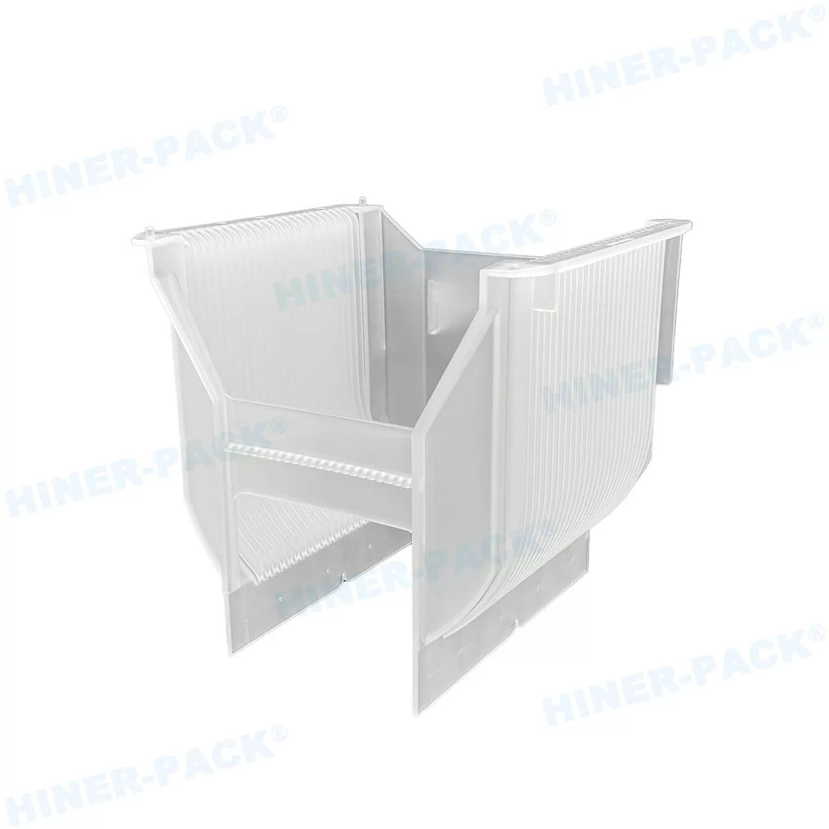
Why Semiconductor Manufacturing Requires Precision Wafer Trays
Modern silicon wafers are thinner and more fragile than ever. As the industry moves toward advanced packaging nodes and thinner substrates, standard carriers no longer offer adequate protection. A single damaged 300mm wafer can cost thousands of dollars in lost yield.
Wafer handling requires specialized carrier media that prevent physical contact with sensitive active areas. Furthermore, automated pick-and-place equipment demands exact dimensional consistency to prevent misalignment jams.
Hiner-pack addresses these critical industry pain points by manufacturing rigid, highly stable wafer packaging. Our trays absorb mechanical shocks while maintaining strict dimensional tolerances under varying operational temperatures.
Core Advantages of Hiner-pack Wafer Trays
When selecting a high-precision wafer tray for sale, engineering specifications matter. Hiner-pack integrates high-grade polymer technology with precise tooling to deliver superior substrate protection.
1. Superior Wafer ESD and Physical Protection
Electrostatic discharge (ESD) remains a silent killer in semiconductor fabrication and assembly. Hiner-pack utilizes custom-blended carbon-filled and conductive polymer compounds to deliver reliable static dissipation.
Controlled Surface Resistivity: Our ESD-safe materials maintain a consistent surface resistivity between 104 and 109 ohms/sq, effectively discharging static without sparking.
Anti-Vibration Pocket Geometry: Specially engineered pocket walls support the wafer along its outer edge, preventing lateral movement during rough transport.
Zero Surface Scratching: Low-friction surface formulations protect delicate anti-reflective coatings and polished wafer backsides from contact abrasion.
2. Secure & Stable Wafer Handling
Automated material handling systems (AMHS) demand absolute dimensional stability. Inconsistent tray dimensions lead to machine downtime, broken wafers, and costly production delays.
Tight Machining Tolerances: Manufactured using ultra-precise molds, ensuring perfect registration with automated robotic grippers.
High Thermal Stability: Our specialized plastics resist thermal deformation, keeping the tray flat during high-temperature baking or cleaning cycles.
Anti-Warpage Construction: Reinforced structural ribbing preserves planar flatness over long-term storage and repeated use cycles.
3. Cleanroom Compatibility & Low Outgassing
Outgassing from low-grade plastics releases volatile organic compounds (VOCs). These airborne molecular contaminants (AMCs) condense on wafer surfaces, causing severe defects during lithography or wire bonding.
High-Purity Raw Materials: We formulate our trays using pure engineering polymers free from silicone, heavy metals, and volatile plasticizers.
Washed in Class 10/100 Cleanrooms: Every wafer tray for sale undergoes rigorous ultrasonic cleaning and vacuum sealing inside our certified cleanroom environments.
Immediate Usability: Trays arrive ready for direct deployment straight into your cleanroom bays without additional pre-washing steps.
4. Reusable & Cost-Efficient Solutions
Managing operational expenditure requires durable packaging that withstands multiple production loops. Hiner-pack designs long-lasting products that drive down Total Cost of Ownership (TCO).
Chemical & Wear Resistance: Strong polymer structures resist degradation from IPA, solvents, and typical fab cleaning agents.
Full-Spectrum Sizes: Available in 2-inch, 4-inch, 6-inch, 8-inch, and 12-inch formats, alongside custom waffle packs for bare die handling.
Turnkey Customization: We offer tailored pocket dimensions, custom lid designs, and laser-engraved serial identification for full traceability.
Why Choose Hiner-pack as Your Semiconductor Partner?
Choosing a reliable supplier for semiconductor packaging requires careful evaluation of technical capability and material consistency. Hiner-pack stands out as a proven industry partner.
Founded in 2013, Hiner-pack has built an extensive R&D network in collaboration with top polymer research institutions. Our engineering team continuously refines conductive composite formulations to meet evolving semiconductor standards.
We hold multiple utility and invention patents focused on ESD protection and precision molding techniques. By managing the complete manufacturing chain—from raw resin compounding to final cleanroom packing—we guarantee strict quality control and competitive lead times.
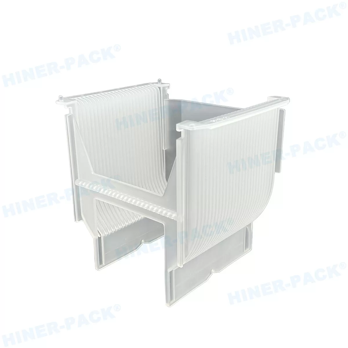
Typical Application Scenarios & Product Specifications
Hiner-pack wafer trays support critical operational workflows across the entire microelectronics manufacturing pipeline:
Semiconductor Wafer Fabs: Safe inter-process transfer and temporary storage of in-process silicon, GaAs, or GaN wafers.
OSAT (Outsourced Semiconductor Assembly and Test) Facilities: Secure placement during automated die bonding, wire bonding, and final testing.
Global Logistics & Shipping: Shock-resistant packaging for international shipping of delicate, ultra-thin polished wafers.
R&D and University Labs: Dust-free, organized storage for specialized research substrates and bare die chips.
Available Product Categories:
2-inch to 12-inch Standard Wafer Trays
Single-Wafer Shipping Containers & Coin-Style Holders
Frame Trays for Diced Wafer Handling
Conductive Waffle Packs for Bare Die and Optical Components
Custom-designed carriers tailored to non-standard substrate shapes
Frequently Asked Questions (FAQ)
Q1: What ESD materials does Hiner-pack use for wafer tray manufacturing?
A1: We utilize conductive polymer blends, including carbon-filled ABS, Polypropylene (PP), PEEK, and Polycarbonate (PC). These materials maintain consistent surface resistivity between 104 and 109 ohms/sq, ensuring long-lasting ESD dissipation that does not wash off or degrade over time.
Q2: Are Hiner-pack wafer trays compatible with automated AMHS equipment?
A2: Yes. Our trays are engineered to match exact international SEMI standards. We manufacture them with tight dimensional tolerances, flat bases, and standardized pickup features, ensuring seamless integration with automated machinery and robotic pick-and-place tools.
Q3: How do you prevent contamination during shipping?
A3: All wafer trays are processed, double-washed via ultrasonic cleaning, and packed inside Class 10 to Class 100 cleanroom environments. They are sealed in static-shielding, low-outgassing moisture barrier bags before leaving our facility.
Q4: Can I request a custom wafer tray for non-standard chip or substrate dimensions?
A4: Absolutely. Hiner-pack offers complete turnkey design services. Our engineering team creates custom mold tooling tailored to your specific substrate dimensions, pocket depths, edge-exclusion requirements, and structural preferences.
Q5: What is the minimum order quantity (MOQ) and lead time when looking for a wafer tray for sale?
A5: We maintain standard sizes in stock for immediate dispatch with flexible MOQs. For customized tray orders, prototype tooling and sample production typically take 2 to 3 weeks, followed by fast bulk production.
Get Your Custom Quote and Samples Today
Are you looking for a reliable, high-precision wafer tray for sale to protect your valuable semiconductor components? Hiner-pack provides cost-effective, high-performance packaging engineered to protect your manufacturing yields.
Contact our engineering specialists today to discuss your technical specifications, request technical datasheets, or order free product samples for trial evaluation.
Direct Email: rainbowzhu@hiner-pack.com / cathyxing@hiner-pack.com
Official Website: www.hiner-pack.com
Protect your silicon assets with Hiner-pack engineering excellence. Submit your RFQ today!














