
In advanced semiconductor manufacturing, where fabrication nodes shrink below 5nm and 3D packaging designs become increasingly complex, the margin for error is virtually non-existent. A single 300mm wafer carrying high-density integrated circuits can reach a value of tens of thousands of dollars. Yet, a common vulnerability in the back-end supply chain lies not in the lithography or etching tools, but in the passive transport vessels that house these wafers during transit and storage. When procurement departments search for reliable wafer carriers for sale, the decision-making process must extend far beyond basic unit price and dimensional compliance.
This guide analyzes the technical requirements of modern wafer packaging. It outlines critical material properties, mechanical considerations for automated handling, and the long-term cost of ownership. By examining these elements, engineering and procurement teams can make informed decisions that protect device yield and maintain process reliability.
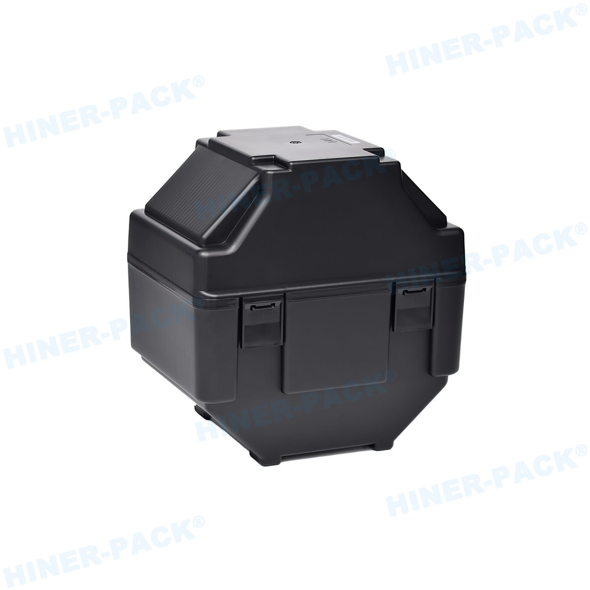
The Outgassing Illusion: Rethinking Contamination in Carrier Sourcing
A frequent oversight in cleanroom procurement is assuming that any carrier molded from standard ESD-safe plastic will suffice for mid-term storage. This assumption overlooks a subtle but damaging phenomenon: molecular outgassing. While visual inspections may show no defects, cheap polymers can release volatile organic compounds (VOCs) over time. These airborne molecular contaminants (AMCs) deposit onto the wafer surface, causing thin-film adhesion failures and shifting threshold voltages during subsequent processing steps.
Data from semiconductor reliability studies indicates that organic contamination on wafer surfaces can reduce packaging yield by up to 3.5% in high-frequency RF and analog device lines. Standard polycarbonate carriers might appear cost-effective initially. However, when evaluating premium wafer carriers for sale, it is essential to request outgassing profiles (GC-MS data) from the manufacturer. This ensures that the material does not compromise the wafer surfaces during transit or long-term warehouse storage.
To address this risk systematically, procurement and process engineering teams can utilize the Hermetic Integrity Triad (HIT) framework. This model evaluates carriers across three interdependent pillars:
Triboelectric Control: Preventing electrostatic discharge through controlled surface resistivity.
Dimensional Rigidity: Maintaining structural tolerances under mechanical load to prevent physical contact with wafer edges.
Outgassing Mitigation: Using low-extractable polymers to prevent micro-contamination of active device areas.
By assessing options through this framework, teams can avoid the pitfalls of low-grade packaging and choose solutions designed for high-yield manufacturing environments.
Material Science: Selecting the Right Polymer for Yield Protection
The performance of a wafer carrier depends heavily on its material composition. When browsing wafer carriers for sale, procurement teams typically choose between three primary classes of polymers: Polypropylene (PP), Polycarbonate (PC), and Polyetheretherketone (PEEK). Each material serves specific operational environments and thermal profiles, as outlined in the comparative table below.
| Material Class | Typical Surface Resistivity (Ω/sq) | Thermal Deformation Temp (°C) | Primary Application | Outgassing Risk |
|---|---|---|---|---|
| Polypropylene (PP) | 109 - 1011 (when carbon-loaded) | 55 - 65 | Short-range transit, inter-bay transfer | Moderate (dependent on additives) |
| Polycarbonate (PC) | 105 - 109 (highly customizable) | 120 - 130 | Automated dry storage, FOSB, FOUP shells | Low to Moderate |
| PEEK / PES | 105 - 108 (stable across temps) | 200 - 260 | High-temp baking, thin wafer processing | Extremely Low |
For standard back-end packaging and shipping, carbon-fiber-reinforced polycarbonate remains a reliable choice. It offers high dimensional stability and impact resistance, keeping wafers secure during domestic and international shipping. For high-temperature processing or thin wafer handling, specialized PEEK carriers are often required to prevent structural warping. The engineering team at Hiner-pack designs customized carrier options that align material specifications with specific process thermal budgets, reducing premature wear and deformation.
Anticipated Procurement Doubt 1: Is PEEK always necessary, or is Polycarbonate sufficient?
A common question when evaluating wafer carriers for sale is whether to invest in expensive PEEK options. The answer depends on your thermal budget and processing chemicals. If your process includes in-carrier baking cycles above 120°C or exposure to aggressive solvents, PEEK is necessary to prevent structural failure. For standard transport, shipping, and ambient-temperature automated storage, carbon-filled polycarbonate provides sufficient physical protection and ESD shielding at a lower capital cost.
Mechanical Compatibility with Automated Material Handling Systems (AMHS)
In modern fab and packaging facilities, manual wafer handling is increasingly rare. Overhead Hoist Transport (OHT) systems and Automated Guided Vehicles (AGVs) rely on precise mechanical interfaces to grip, lift, and deposit wafer carriers. Therefore, evaluating wafer carriers for sale requires verifying strict adherence to SEMI standards (such as SEMI E1.9, E15.1, and M31).
If a carrier deviates from these dimensional specifications by even a fraction of a millimeter due to structural warping or manufacturing variances, automated systems can misalign. This misalignment can cause robot handling errors, automated process stoppages, or wafer breakage inside the load port. Robust carrier designs incorporate reinforced top flanges, stable kinematic couplings, and side-lifting notches that resist deformation over repeated cycles of robotic handling.
Anticipated Procurement Doubt 2: How do carriers handle wear from automated systems?
Purchasing managers often wonder how robotic handling affect carrier longevity. While high-impact polymers withstand repeated robotic gripping, microscopic wear particles can accumulate over time. To minimize contamination risks, select carriers with reinforced wear plates at key contact points. High-quality wafer carriers for sale from experienced suppliers like Hiner-pack are engineered to limit particulate generation during mechanical interface cycles, protecting both the wafers and the automated handling equipment.
Sourcing Smart: Calculating Total Cost of Ownership (TCO)
The initial purchase price of a wafer carrier is only a portion of its actual cost over its operational lifespan. A low-cost carrier that warps after five wash cycles or sheds particles during transport can quickly become expensive due to yield loss and line downtime. A comprehensive evaluation of wafer carriers for sale should calculate the Total Cost of Ownership (TCO) using the following formula:
TCO = (Unit Acquisition Cost + Cleaning/Maintenance Costs) / (Expected Lifecycle Cycles * Average Yield Rate)
This metric highlights why investing in durable carriers can be more economical over time. High-quality carriers designed for repeated washing cycles, resistant to surfactant degradation, and stable against UV exposure offer a longer service life. Over hundreds of process runs, a durable carrier can lower the cost-per-transfer and improve long-term yield stability.
Anticipated Procurement Doubt 3: Can recycled plastics meet sustainability targets?
With growing interest in corporate ESG initiatives, packaging engineers often ask if recycled materials are suitable for wafer transport. For primary wafer contact carriers, virgin, semiconductor-grade resins remain necessary due to strict contamination limits. However, recycled materials can be used for secondary protective packaging, such as outer shipping shells or non-contact storage components, allowing facilities to support sustainability initiatives without risking wafer contamination.
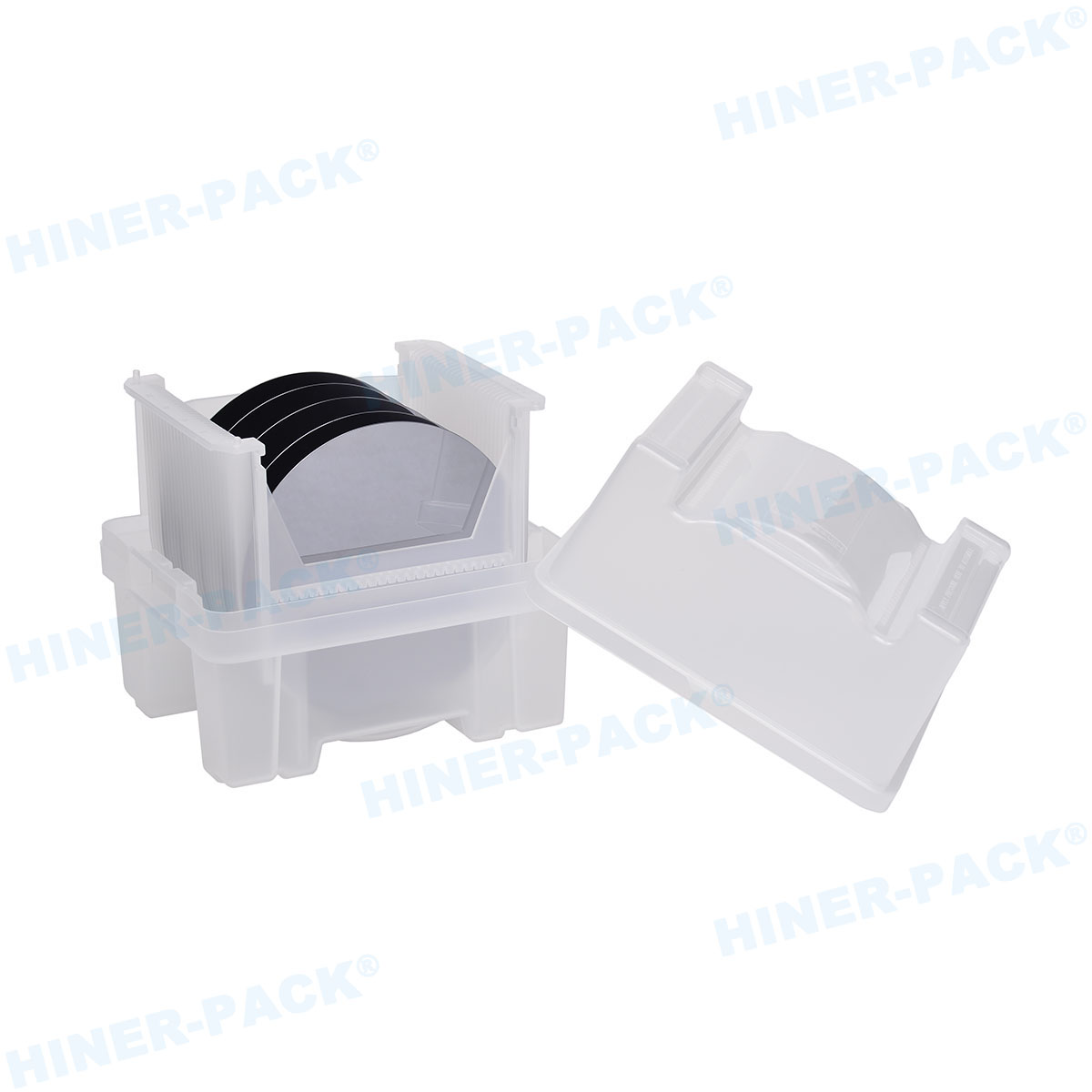
Technical Procurement Checklist for Wafer Carriers
Before finalizing an RFQ for wafer carriers for sale, engineering and purchasing teams can use this practical checklist to verify essential requirements:
Material Certification: Request cleanroom-grade polymer documentation with trace metal and outgassing analysis.
ESD Protection: Verify surface resistivity remains within the dissipative range (105 to 109 Ω/sq) across the entire carrier body.
Standard Compliance: Confirm adherence to relevant SEMI standards for automated handling and load-port interfaces.
Chemical Compatibility: Ensure the carrier can withstand standard cleanroom detergents, isopropyl alcohol (IPA), and ultrasonic cleaning processes.
Thermal Stability: Confirm the carrier maintains dimensional stability at your facility's maximum storage or drying temperatures.
Vendor Support: Choose partners who provide technical support, custom design options, and post-sale engineering services, such as Hiner-pack.
Frequently Asked Questions
Q1: What is the recommended cleaning interval for wafer carriers in a
standard cleanroom?
A1: Cleaning intervals depend
on your facility's cleanroom class and process steps. Typically, carriers used
for inter-bay transport in Class 100 (ISO 5) environments should be washed after
every 5 to 10 cycles. For long-term storage or shipping, carriers must undergo a
verified wash and dry cycle before loading new wafers.
Q2: How does ESD-safe plastic prevent damage to sensitive
ICs?
A2: ESD-safe plastics contain conductive
additives (such as carbon powder or carbon fibers) that lower surface
resistivity. This allows static charges to dissipate safely to the ground rather
than accumulating and causing a rapid electrostatic discharge that could damage
wafer circuitry.
Q3: Why is dimensional stability important when sourcing wafer
carriers for sale?
A3: Automated tools use precise
sensors to locate wafer slots. Even minor warping in the carrier structure can
cause robotic arms to misalign, leading to scratched wafers or handling errors
that interrupt production.
Q4: Can these carriers be customized for non-standard wafer
thicknesses?
A4: Yes. While standard carriers are
designed for typical SEMI-specified thicknesses, custom carriers are available
for thin, thick, or bonded wafers. Working with manufacturers like Hiner-pack allows you to
customize slot widths, pitches, and support structures for unique process
requirements.
Q5: What is the typical lifespan of a premium wafer shipping
box?
A5: Under normal handling and standard
cleaning protocols, premium polycarbonate or high-durability polypropylene
carriers can complete 50 to 100 round-trip shipments before physical wear or
micro-scratches require replacement.
Selecting the right packaging solutions is critical to protecting wafer quality and ensuring smooth operations. Evaluating wafer carriers for sale requires looking beyond the initial purchase price to consider material properties, structural integrity, and automated system compatibility. To explore engineered options that meet cleanroom standards, visit the product lineup at Hiner-pack and contact our technical support team to discuss your specific requirements.














