
In semiconductor manufacturing, transporting and storing silicon wafers requires an environment that preserves absolute purity and structural integrity. As integrated circuit feature sizes shrink below the 5-nanometer threshold, even sub-micron particulates or molecular outgassing can lead to severe yield losses. Safely moving these fragile substrates between front-end fabs and back-end assembly facilities depends entirely on specialized transport containers, such as Front Opening Unified Pods (FOUPs), Front Opening Shipping Boxes (FOSBs), and wafer cassettes. Partnering with a highly qualified wafer carriers factory ensures that these transport systems meet the exact tolerances and cleanliness protocols required by modern fabs.
For B2B procurement managers and packaging engineers, evaluating a manufacturing partner involves assessing material science expertise, cleanroom production capabilities, and adherence to international semiconductor standards. As a specialized manufacturer in this field, Hiner-pack designs high-performance packaging and shipping systems engineered to protect wafers throughout their operational lifecycle.
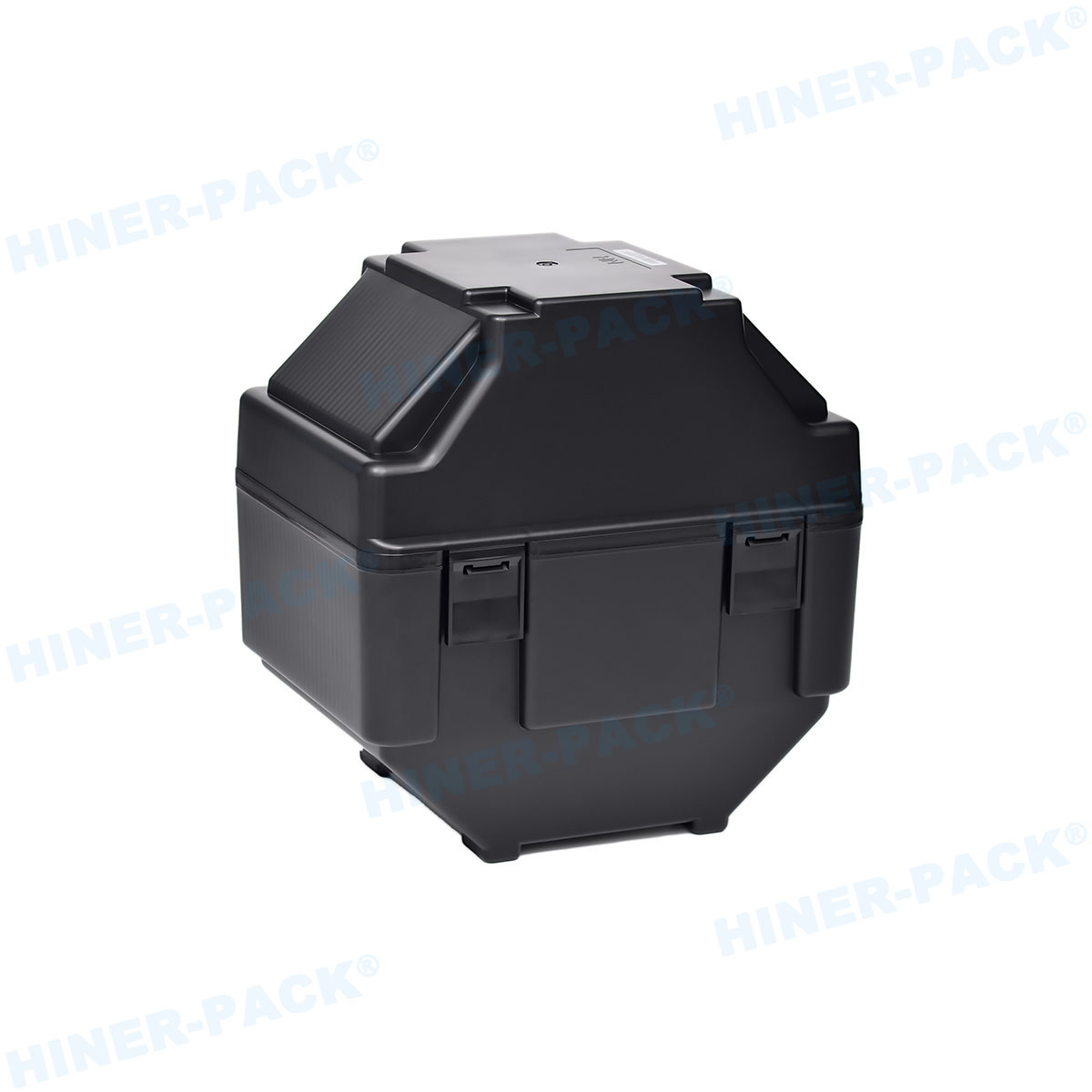
1. Contamination Risks and Physical Stress in Wafer Logistics
During transport, silicon wafers are vulnerable to environmental and mechanical hazards. To mitigate these risks, the structural design of a wafer carrier must address three primary vectors of damage: airborne molecular contamination, static discharge, and mechanical vibration.
Airborne Molecular Contamination (AMC)
AMCs consist of volatile organic compounds (VOCs), acids, bases, and dopants present in the surrounding air or released by packaging materials. If a carrier utilizes low-grade polymers, these materials can release gases over time. These outgassed molecules deposit onto the clean silicon surface, forming microscopic films that disrupt subsequent deposition, lithography, or etching steps. Minimizing AMC requires the use of specialized, ultra-low-outgassing polymers that have been baked and verified in controlled environments.
Electrostatic Discharge (ESD)
Silicon is highly sensitive to static accumulation. Standard insulating plastics can generate significant triboelectric charges during transport, handling, or machine loading. A sudden discharge can puncture thin oxide layers or attract airborne particulates to the wafer surface via electrostatic attraction. Consequently, materials must feature controlled electrostatic dissipative (ESD) properties, maintaining a precise surface resistivity range to safely bleed off static charges without causing sudden electrical transfers.
Mechanical Stress and Vibration
During inter-facility shipping, micro-vibrations can cause the wafers to rub against the internal pocket walls of the carrier. This friction generates particulate contamination, commonly known as "pocket wear particles." Furthermore, sudden shocks can lead to micro-fractures along the crystal lattice of thinned wafers, leading to wafer breakage during subsequent high-temperature fab steps. Well-designed internal support combs and shock-absorbing structures are necessary to dampen these external forces.
2. Polymer Engineering in a Wafer Carriers Factory
The performance of a wafer carrier depends heavily on the polymer formulation selected for its construction. A professional wafer carriers factory must possess deep material science expertise to select, compound, and injection-mold advanced engineering plastics that meet both chemical resistance and mechanical strength requirements.
| Polymer Type | Key Characteristics | Primary Applications |
|---|---|---|
| PEEK (Polyetheretherketone) | Extreme thermal stability, high wear resistance, ultra-low outgassing, high rigidity. | Process cassettes, high-temperature transport, robotic alignment structures. |
| PFA (Perfluoroalkoxy) | Exceptional chemical inertness, high purity, resistance to strong acids/solvents. | Wet processing, chemical etching cassettes, cleaning bath carriers. |
| Carbon-Filled PC (Polycarbonate) | Excellent dimensional stability, mechanical impact resistance, tailored ESD conductivity. | FOSB bodies, shipping box shells, structural frames. |
| PP (Polypropylene) | Ductile, cost-efficient, chemical resistance to mild agents, lightweight. | Internal shipping cushions, low-stress storage containers. |
By compounding these base resins with carbon fibers, carbon powder, or proprietary antistatic agents, raw material suppliers and manufacturers can fine-tune the electrical and mechanical characteristics of the carrier. For instance, carbon-fiber-reinforced PEEK is widely used in automated material handling systems (AMHS) due to its structural stiffness and low friction coefficient, which prevents particle generation during rapid automated loading cycles.
3. Key Manufacturing Processes and Cleanroom Protocols
Production quality is determined by the control systems implemented within the manufacturing facility. Fabricating high-purity carrier systems requires specialized tooling, advanced injection molding machines, and ISO-certified cleanroom environments.
Precision Injection Molding
The structural parts of wafer carriers are produced using high-clamping-force injection molding machines. Because polymers like PEEK and PFA require high melt temperatures, the molds must feature advanced heating and cooling channels to ensure uniform thermal distribution. Any thermal variance during the cooling phase can introduce molded-in stress, resulting in structural warpage. A warped carrier cannot sit flat on a process tool's load port, which can trigger sensor faults or cause robot handling systems to misalign.
ISO Class 4 and Class 5 Cleanroom Assembly
Post-molding operations, including structural assembly, gasket installation, and final inspection, must occur in a highly controlled environment. A reputable wafer carriers factory maintains ISO Class 5 (Class 100) or ISO Class 4 (Class 10) cleanrooms. Technicians in full cleanroom suits assemble the carriers, ensuring that no human-derived skin flakes, hair, or fibers contaminate the interior pockets.
Deionized Water Cleaning and Outgassing Control
Before packaging, completed carriers undergo multi-stage ultrasonic cleaning cycles using Ultra-Pure Water (UPW) with a resistivity of 18.2 Megohm-cm. This process removes surface particles and trace ionic contaminants. Following the wash cycle, carriers are dried using heated, ultra-high-purity nitrogen gas (N2) or undergo vacuum baking to extract residual moisture and volatile organic compounds from the polymer matrix. By managing these parameters, Hiner-pack ensures that every carrier meets strict cleanliness requirements before shipment.
4. SEMI Standards Compliance and Dimensional Tolerance
The semiconductor industry relies on automated material handling systems (AMHS) to move wafers between process chambers. To guarantee seamless integration with tools from different equipment manufacturers, wafer carriers must comply with strict global standards established by the SEMI (Semiconductor Equipment and Materials International) organization.
SEMI E1.9 (FOSB Specification): Outlines the physical dimensions, mechanical interfaces, and latching mechanisms for 300mm Front Opening Shipping Boxes, ensuring compatibility with automated load ports.
SEMI E110 (Specification for FOUP): Defines the interface requirements for front-opening unified pods used in highly automated 300mm fabs, focusing on kinematic coupling pins and automated door opening mechanisms.
SEMI M31 (Specification for Wafer Cassettes): Governs the dimensions of cassettes used to hold 150mm and 200mm wafers, focusing on slot pitch, pocket depth, and alignment notches.
To meet these standards, a wafer carriers factory must use highly precise coordinate measuring machines (CMMs) and optical measurement systems to verify structural tolerances down to the micron level. Key dimensions, such as the pitch between wafer slots, must be kept within tight tolerances. A deviation of just a fraction of a millimeter can cause robot vacuum wands to scrape the wafer surface during pick-and-place operations, leading to scratched active areas or chipped wafer edges.
5. Solving Modern Packaging Challenges: Thin Wafers and Chiplets
As the semiconductor industry adopts 2.5D/3D integration, chiplets, and wafer-level packaging (WLP), wafer carrier requirements are shifting. Standard carriers designed for rigid, 775-micron-thick silicon wafers are no longer sufficient for these specialized applications.
Ultra-Thin Wafer Handling
Wafers thinned down to 100 microns or less for high-bandwidth memory (HBM) stacking are extremely fragile and prone to warping. Standard gravity-fed vertical cassettes can cause thinned wafers to bow, leading to structural damage or escape from the slots during transit. Specialized shipping boxes incorporate customized backing rings, coin-set coin-stack structures, or protective interleaving liners to gently secure the thinned silicon without applying concentrated mechanical pressure.
Reconstituted Wafer Transport
In Fan-Out Wafer-Level Packaging (FOWLP), wafers are reconstructed using individual dies embedded in an epoxy mold compound. These reconstituted wafers often exhibit high warpage due to mismatches in thermal expansion coefficients between the silicon and the molding compound. To accommodate this, wafer carriers require deeper slots, modified mechanical retention gates, and specialized ESD-safe materials that prevent static generation on both the silicon and organic mold surfaces.
Solving these advanced challenges requires close collaboration with an engineering-focused manufacturer like Hiner-pack, which provides tailored carrier configurations and custom-engineered injection-molded components designed for non-standard wafer geometries.
6. Procurement Best Practices: Conducting a Factory Audit
When selecting a manufacturing partner for long-term wafer carrier supply, B2B procurement professionals should look beyond unit prices and focus on quality consistency and engineering capabilities. A thorough factory audit should evaluate several operational areas:
Raw Material Traceability: Ensure the factory maintains complete batch traceability for all engineering resins. Virgin resin materials should never be blended with unverified regrind plastics for high-purity carrier applications.
Cleanroom Maintenance: Review daily records of airborne particle counts, relative humidity, and temperature stability inside the cleaning and assembly cleanrooms.
Metrology and Testing Equipment: Verify that the factory has on-site coordinate measuring machines (CMM), surface resistivity meters, outgassing analysis systems (such as GC-MS), and liquid particle counters (LPC) to monitor washing water purity.
Scalability and Tooling Maintenance: Confirm that the factory possesses the tooling capacity to scale production volumes quickly and has regular preventative maintenance schedules for its high-injection molds.
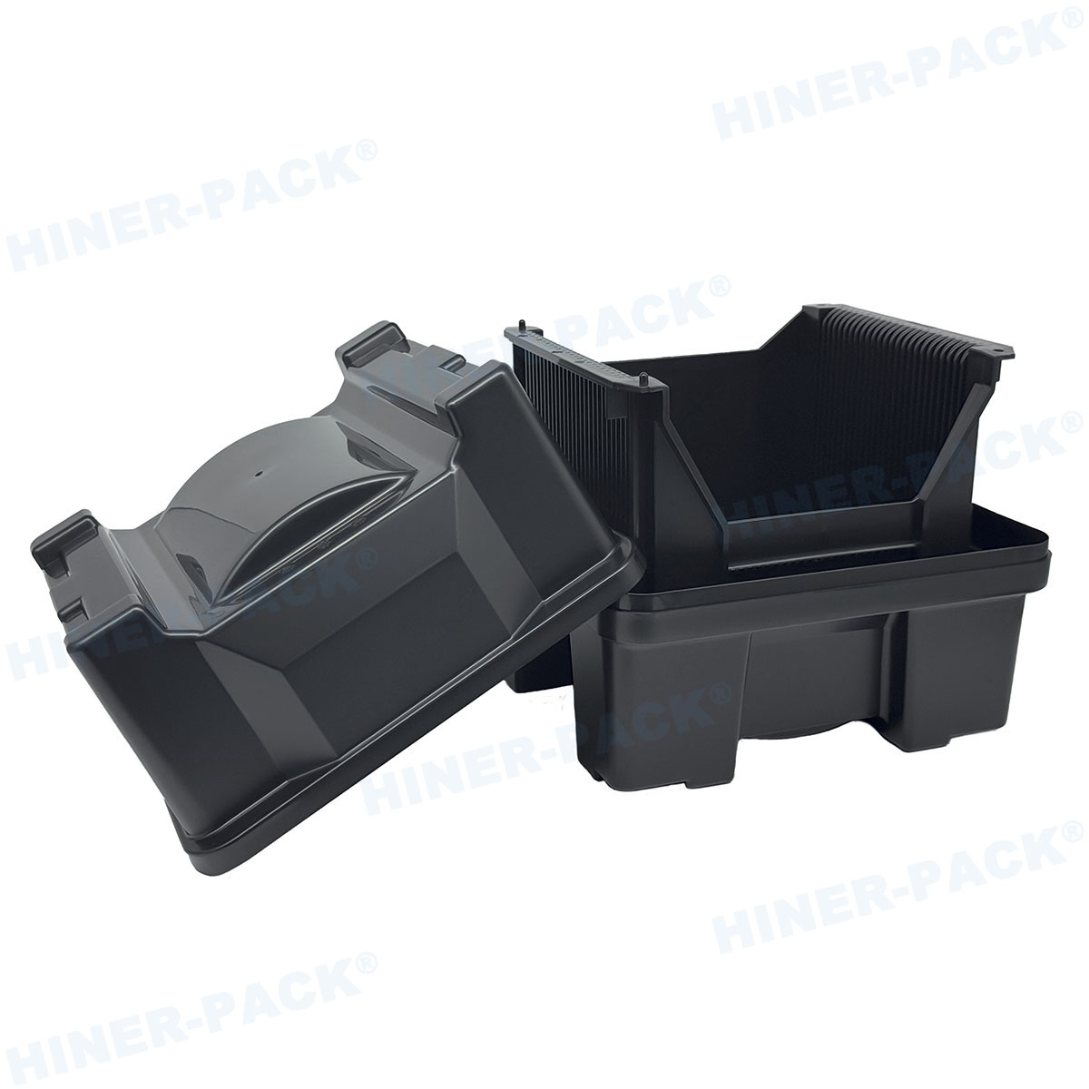
Conclusion and Inquiry Invitation
The wafer carrier is a key component in protecting semiconductor assets during transport and processing. Selecting a professional wafer carriers factory ensures your wafers are protected against micro-contamination, electrostatic discharge, and mechanical shock. By prioritizing material science, cleanroom processing, and SEMI compliance, wafer manufacturers can optimize process yields and minimize transit losses.
If you are looking to upgrade your wafer shipping infrastructure, design a custom transport cassette for thin wafers, or request detailed material outgassing reports, contact our engineering team today. Send us your project specifications, and we will provide customized drawings and evaluation samples for your evaluation.
Contact Hiner-pack to Request a Quote
Frequently Asked Questions (FAQ)
Q1: Why is Polycarbonate (PC) preferred for shipping boxes but PEEK for process cassettes?
A1: Polycarbonate offers high impact resistance, dimensional stability, and can be made clear or ESD-safe, making it suitable for shipping boxes (like FOSBs) that protect wafers from external impacts. However, PC cannot withstand the high temperatures and harsh chemical environments of wet etching or deposition. PEEK is chosen for process cassettes because it maintains its structural integrity above 120°C, exhibits superior chemical resistance, and has exceptionally low wear-particle generation during automated handling.
Q2: How does a wafer carriers factory control ESD properties?
A2: Manufacturers control ESD properties by compounding virgin polymers with conductive elements, such as carbon fiber, carbon powder, or non-sloughing inherently dissipative polymers (IDPs). This process targets a surface resistivity between 105 and 109 ohms per square. This range is conductive enough to bleed off static safely, but resistive enough to prevent rapid, spark-inducing electrical discharges.
Q3: What is the significance of SEMI compliance for wafer cassettes?
A3: SEMI compliance ensures that wafer cassettes, FOSBs, and FOUPs fit perfectly with automated load ports, robot grippers, and overhead hoist transport (OHT) systems used in fabs. Without strict adherence to standards like SEMI E1.9 or E110, automated systems could fail to align with the carrier, leading to handling errors, wafer dropping, or system downtime.
Q4: How do cleaning protocols differ between shipping boxes and in-process cassettes?
A4: Shipping boxes focus on removing surface particulates, moisture, and VOCs that accumulate during transport. In-process cassettes, which are exposed to aggressive chemicals and high temperatures, require deeper cleaning processes. This includes multi-stage ultrasonic cleaning with ultra-pure water (UPW) and hot nitrogen drying to remove trace ionic contaminants, heavy metal residues, and chemical surfactants before they enter clean process tools.
Q5: Can customized wafer carriers be engineered for non-silicon substrates like SiC or GaN?
A5: Yes. Silicon Carbide (SiC) and Gallium Nitride (GaN) wafers are typically heavier, harder, and have different transparent properties than standard silicon. A professional manufacturer can modify pocket depths, slot spacing, and material formulations to support these dense, fragile compound semiconductors and prevent pocket chipping during transport.














