
In semiconductor wafer-level packaging and backend fabs, the wafer carriers price often becomes a point of contention between procurement teams and process engineers. A low-bid carrier might save upfront dollars but risk wafer damage, particle contamination, or automation incompatibility. Over the past decade consulting for OSATs (Outsourced Semiconductor Assembly and Test) and IDMs, I have observed that true cost-efficiency lies in understanding why prices vary—material science, dimensional control, surface resistivity, and application-specific design. This guide breaks down each factor, providing an authoritative framework for evaluating wafer carriers price without falling into simplistic “per-unit” traps. We will also explore how engineering-grade solutions from Hiner-pack align technical specifications with operational realities.
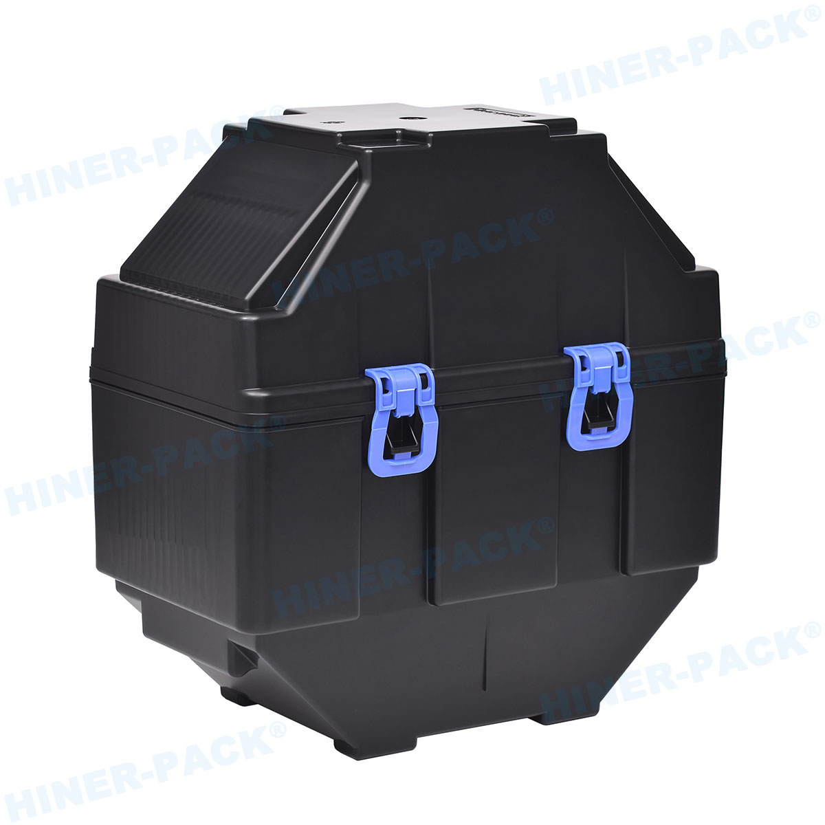
1. Material Selection as the Primary Driver of Wafer Carriers Price
The base polymer defines nearly 40–60% of the final wafer carriers price. High-volume fabs handling 200mm and 300mm wafers commonly encounter three material families: PEEK (polyether ether ketone), PES (polyethersulfone), and PPS (polyphenylene sulfide) blended with static-dissipative additives. Each offers distinct thermal, mechanical, and electrostatic discharge (ESD) performance, directly influencing cost.
PEEK-based carriers: Exceptional thermal stability (continuous use up to 260°C) and chemical resistance. Ideal for backend processes like curing or die attach films. However, raw PEEK resin is 5–7× more expensive than standard engineering plastics. A 300mm PEEK wafer carrier typically commands premium pricing, but it withstands hundreds of autoclave cycles without warpage.
PES and PEI (Ultem) carriers: Good thermal capability (180–210°C) and lower cost than PEEK. Frequently selected for temporary bonding/debonding applications. The trade-off: slightly higher moisture absorption, which may affect dimensional stability in humid cleanrooms.
PPS/PP-based antistatic carriers: Lowest cost tier, suitable for room-temperature storage and transport. However, they degrade rapidly under temperatures above 120°C or aggressive solvents like NMP. Many suppliers quote low wafer carriers price using these materials, but process compatibility must be validated.
Additionally, the method of introducing conductivity matters. Surface-coated carriers are cheaper but prone to coating flaking (particle risk). Bulk-loaded carbon/CNT compounds increase base resin cost but provide permanent, uniform ESD protection. When comparing wafer carriers price across vendors, request material datasheets confirming surface resistivity (10⁶–10⁹ Ω/sq) and temperature rating.
2. Dimensional Tolerances and Design Complexity – Precision Costs Money
Wafer carriers are not passive trays; they are precision alignment tools. For automated wafer handling (robotic end effectors, EFEMs, and sorter systems), slot-to-slot pitch tolerance must stay within ±0.05 mm, and overall flatness under 0.1 mm across 300mm carriers. Achieving these specifications requires:
High-cavitation injection molds with hardened steel cores (tooling cost $15k–$40k per carrier type).
In-line coordinate measuring machine (CMM) inspection for every batch.
Stress-relief annealing post molding to avoid warpage.
Customized designs—such as thin-wafer support ribs, edge-grip features for ultra-thin wafers (below 100µm), or RFID slots for tracking—add non-recurring engineering (NRE) charges that influence the unit wafer carriers price. Conversely, standard JEDEC-compliant carriers enjoy amortized tooling across the industry. Always ask: “Is the quoted price based on existing tooling or new development?”.
For advanced packaging like fan-out wafer-level packaging (FOWLP), carriers require specific fiducial marks and vacuum channels. The added complexity directly elevates wafer carriers price by 20–40% compared to baseline shipping carriers. Yet, failing to meet these tolerances leads to wafer-edge chipping or misalignment during compression molding—a far larger loss.
3. Cleanroom Compatibility & Contamination Control Specs
Semiconductor fabs operate under ISO Class 4 or 5 cleanrooms (Class 10/100). Wafer carriers must be produced, assembled, and packaged in equivalent environments. Not all suppliers maintain this discipline. Key contamination-related price drivers include:
Molding in ISO Class 6 or better: Lower-class rooms require HEPA filtration, gowning protocols, and air shower interlocks—operational costs that reflect in the final price.
Post-molding cleaning: Ultrasonic deionized water + surfactant baths, followed by hot-air drying in laminar flow. Some low-cost vendors skip cleaning, leaving mold-release residues.
Individual cleanroom bagging: Double-bagged with vacuum-sealed ESD shielding. Packaging alone adds $1–$3 per carrier.
Particle count certification: Laser particle counter testing for ≥0.1µm particles. Reliable reports cost overhead but are mandatory for 300mm advanced nodes.
When you see a suspiciously low wafer carriers price, request particle test data according to SEMI G71 or ISO 14644-14. Reputable manufacturers like Hiner-pack provide lot-specific cleanliness certificates, ensuring no contamination-induced yield loss.
4. Wafer Size, Thickness, and Extreme Process Temperatures
The physical geometry of wafers directly maps to carrier design stress points. Key variables impacting engineering and thus wafer carriers price are:
Wafer diameter: 150mm carriers are simpler and lower-cost (mold smaller, less material). 300mm carriers require larger platens, more sophisticated cooling channel design to avoid sink marks, and heavier handling automation. The price difference between 200mm and 300mm standard carriers often ranges 50–80%.
Ultra-thin wafers (50–150µm): Special “low bow” carrier geometry with increased support points and reduced slot depth. Warpage control demands advanced simulation (FEA) and iterative prototyping, driving NRE upward.
High-temperature processes (>220°C): Many fan-out and wafer bonding processes involve thermal cycles above 250°C. Only PEEK or specially formulated PEI carriers survive without creep. Such materials amplify the base wafer carriers price.
Additionally, some 300mm carriers are designed for FOUP-like interfaces (ISO standards). These include kinematic coupling pins and front opening features, adding injection molding complexity. Evaluate your specific process flow: does your carrier need to endure thermal shocks, or is it strictly for inter-bay transport? Matching application severity avoids both overpaying for unnecessary features and under-engineering.
5. Custom Engineering, NRE, and Volume Amortization
Many semiconductor lines migrate from standard to semi-custom wafer carriers due to unique equipment interfaces or thin-wafer requirements. The NRE costs involved—CAD design, mold flow analysis, prototype injection runs, and mechanical qualification—can range $8,000 to $30,000 per carrier family. How this NRE is amortized dramatically affects unit wafer carriers price:
Low-volume (100-500 units/year): NRE amortization heavily inflates per-piece price; request a separate NRE line item to keep future recurring costs predictable.
Mid-to-high volume (>2000 units/year): Spread NRE over larger batches—wafer carriers price becomes more material-and-cycle-time driven.
Exclusive tooling ownership: Some suppliers discount NRE but increase per-unit price; others amortize NRE over a defined contract. Transparency is key.
Leading suppliers such as Hiner-pack offer modular carrier platforms that share common bases and interchangeable inserts, reducing both NRE and unit price across multiple wafer sizes. During procurement, ask about reusing existing mold bases—this can lower your customized wafer carriers price by 25–35% without compromising specifications.
6. Evaluating Supplier Quality Systems & Long-Term Reliability
A low wafer carriers price loses its appeal if carriers delaminate, lose ESD effectiveness after 50 cleaning cycles, or suffer from dimensional drift after thermal aging. Professional buyers should request:
Cleanroom validation report (particle, outgassing by GC-MS).
Warpage data after temperature cycling (−40°C to 150°C, 10 cycles).
Wear resistance: Surface roughness change after 1000 simulated wafer insertion/removal cycles.
Lot traceability: Each carrier labeled with mold cavity number and date code for root-cause analysis.
From my field experience, OSATs that select carriers solely based on initial wafer carriers price often encounter three hidden drains: increased particle monitor counts, scratch defects on wafer backside, and robot end-effector misfeed events. These operational setbacks far exceed any 15% savings in carrier sourcing. Instead, adopt a technical qualification matrix where weight is given to material certifications, tolerances, and supplier process control.
Furthermore, consider the carrier’s cleanability—carriers that degrade after standard IPA or DI water rinses force frequent replacement, raising long-term expenditure. Always test a sample batch (25–50 carriers) in your actual production environment before committing to volume pricing.
Summary: Structuring Your Wafer Carrier Procurement Approach
To properly benchmark wafer carriers price, decompose each quote into four components: raw material grade, manufacturing precision/certifications, NRE amortization, and packaging/logistics. Avoid comparing “apples-to-oranges” where one supplier includes cleanliness certification and another does not. For advanced nodes (≤28nm and beyond), particle control alone justifies paying a premium. Conversely, for legacy 150mm storage applications, a standardized polycarbonate carrier with minimal certifications may be entirely adequate.
Leading suppliers like Hiner-pack provide transparent engineering breakdowns, allowing you to see exactly what drives the quoted wafer carriers price and where adjustments can be made. Collaborating early in the design phase results in optimal balance between performance and cost—avoiding both over-engineering and field failures.
Frequently Asked Questions (FAQ)
Q1: What is the typical wafer carriers price range for a standard 300mm antistatic PES carrier (non-heated applications)?
A1: For a baseline 300mm PES carrier with surface resistivity 10⁶–10⁹ Ω/sq, produced in ISO Class 7 environment without individual particle certification, unit prices typically range from $45 to $85 per piece in volumes of 500–2000 units. Adding SEMI-compliant particle testing and cleanroom double-bagging increases the range to $70–$120. Keep in mind that high-thermal PEEK versions start from $150+ per carrier.
Q2: How does carrier customization affect lead time and wafer carriers price for thin-wafer (100µm) handling?
A2: Custom thin-wafer carriers require FEA simulation to optimize rib patterns and slot depths. Typical NRE ranges $12,000–$22,000 with a lead time of 10–14 weeks for first articles. The unit price after tooling amortization may be 30–50% higher than standard catalog carriers due to lower molding cycles (more careful ejection) and 100% inspection for flatness. For urgent needs, some suppliers, including Hiner-pack, offer rapid prototyping with CNC-machined carriers (higher per-unit cost but zero NRE).
Q3: Are there hidden costs that suppliers exclude from the wafer carriers price quote?
A3: Yes. Common exclusions include: ① Validation samples (may be charged separately), ② Export crating for air freight (especially for large 300mm carriers), ③ Re-qualification fees if design changes later, ④ Mold maintenance fees for high-volume contracts. Always request a full breakdown including NRE, sample costs, packaging for cleanroom transfer, and minimum order quantity (MOQ) implications. A transparent supplier will itemize these.
Q4: Can I use low-cost PP carriers for high-temperature curing processes to save on wafer carriers price?
A4: Not recommended. Polypropylene (PP) has a glass transition temperature around 100°C; above that, carriers soften and permanently warp, potentially damaging wafers or causing misalignment in convection ovens. For processes exceeding 120°C, use at minimum PES or PEI. Although the initial wafer carriers price is higher, preventing just one scratched wafer lot (worth thousands of dollars) justifies the material upgrade. Always match the carrier’s heat deflection temperature (HDT) to your peak process temperature plus a 20°C safety margin.
Q5: Does Hiner-pack provide engineering support to optimize wafer carriers price for specific fab automation lines?
A5: Absolutely. Hiner-pack offers design-for-manufacturing reviews, 3D scanning of existing equipment interfaces, and material recommendations to minimize NRE while maintaining performance. They work with customers to adjust features—such as reducing unnecessary ribs or optimizing gate locations—to lower cycle times and thus unit wafer carriers price without compromising mechanical integrity. Contact their engineering team for a consultation.
Q6: How many cleaning cycles should I expect from a standard ESD-safe wafer carrier before static performance degrades?
A6: Carriers with surface coatings (spray-on antistatic) often degrade after 50–100 cleanings in IPA or DI water. For bulk-loaded conductive compounds (carbon/CNT), ESD performance remains stable for 500+ cycles, provided no aggressive solvents attack the polymer matrix. This longevity directly affects total procurement value. When comparing wafer carriers price, ask for documented cleaning cycle test data—a cheaper coated carrier may need replacement three times as often as a slightly more expensive molded-in conductive version.
Need
a detailed quotation or engineering recommendation on wafer carriers price for
your specific wafer size, process temperature, and automation line? Submit your inquiry to our technical sales team. We will respond with a
specification-based cost breakdown and sample qualification plan.
Send us an inquiry now — discuss your requirements with
Hiner-pack’s semiconductor packaging specialists and secure the optimal balance
of performance, reliability, and value.














