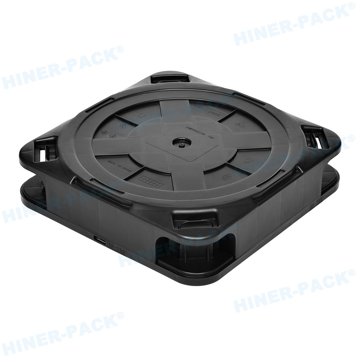
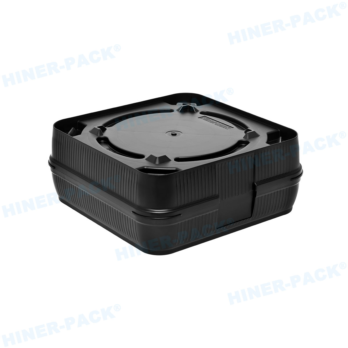
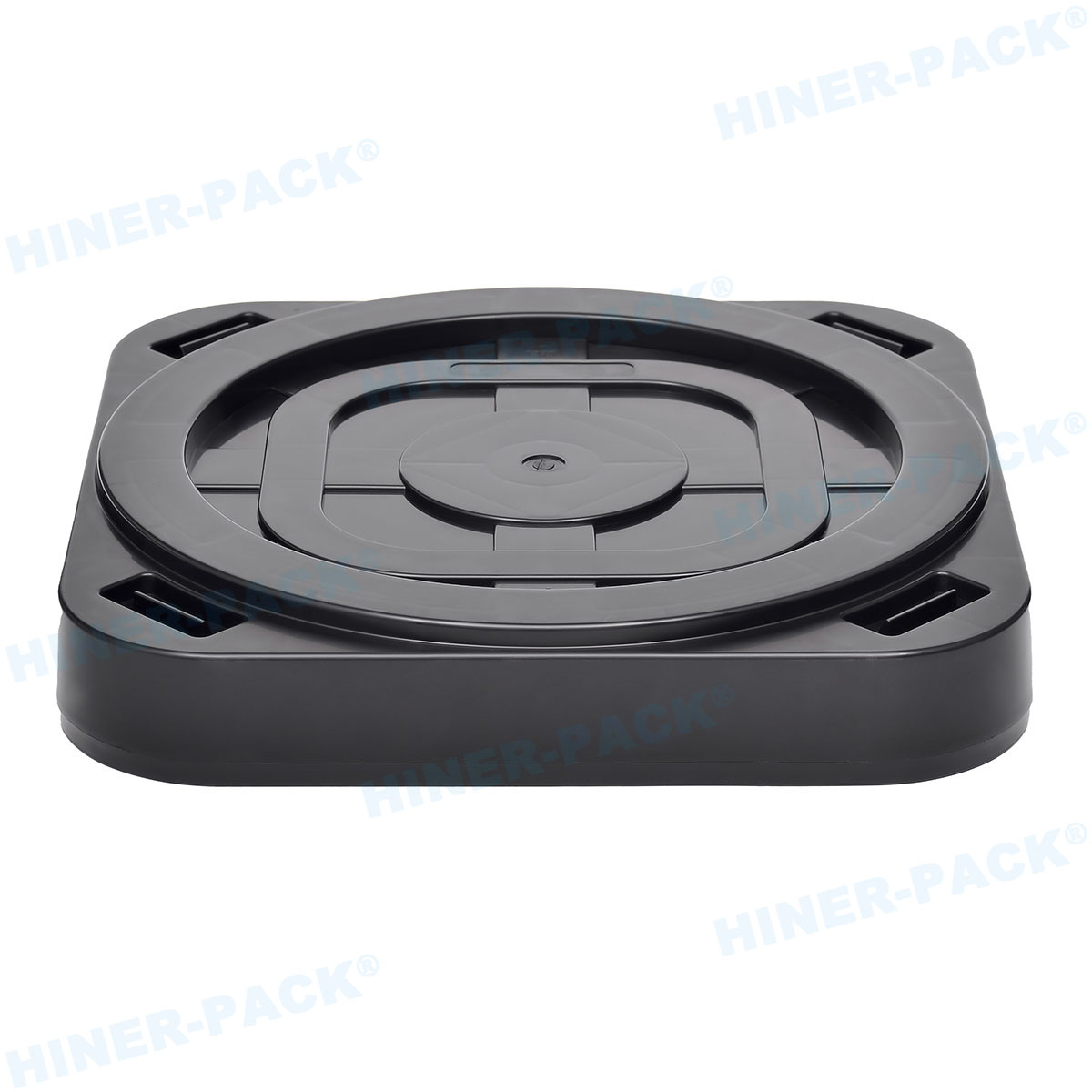
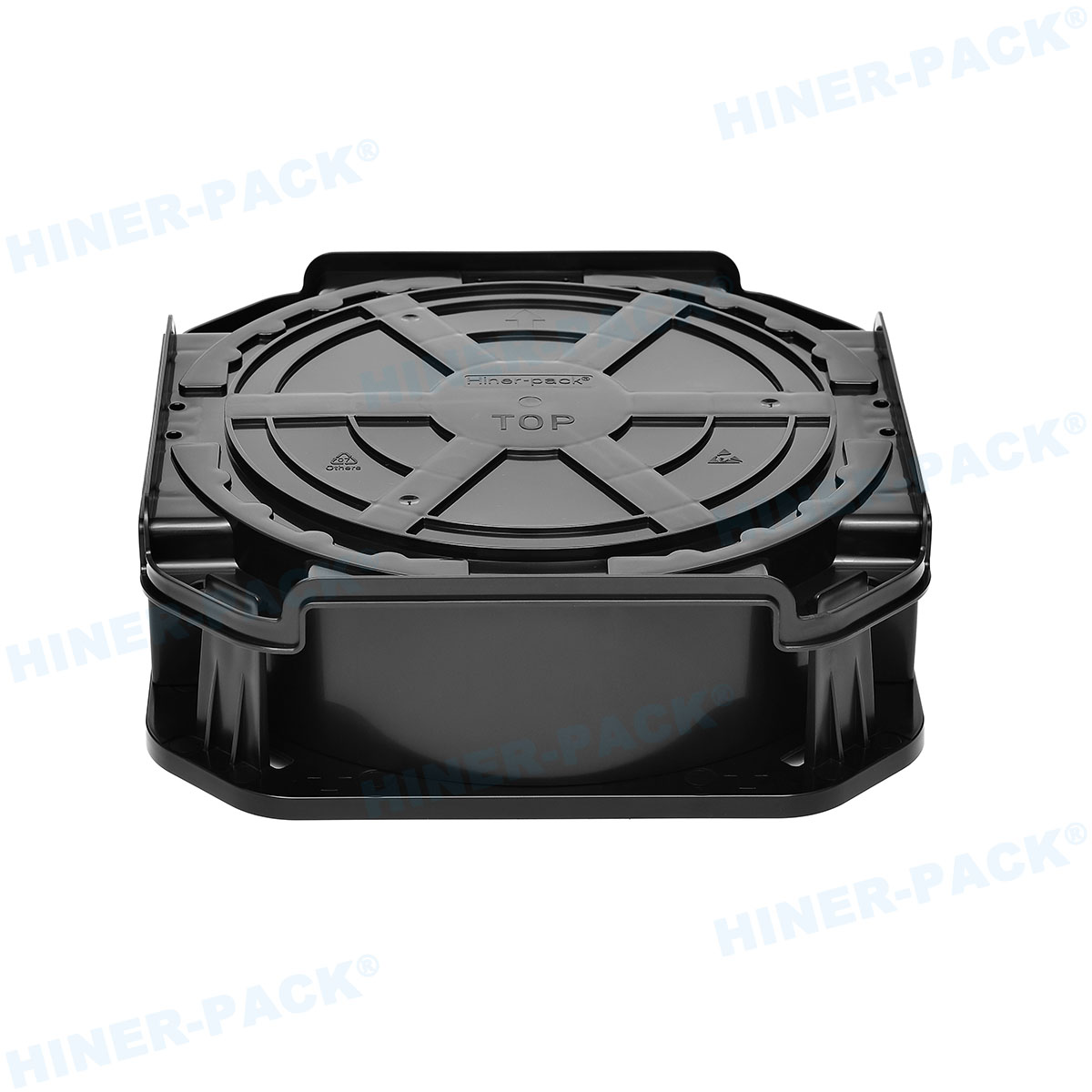
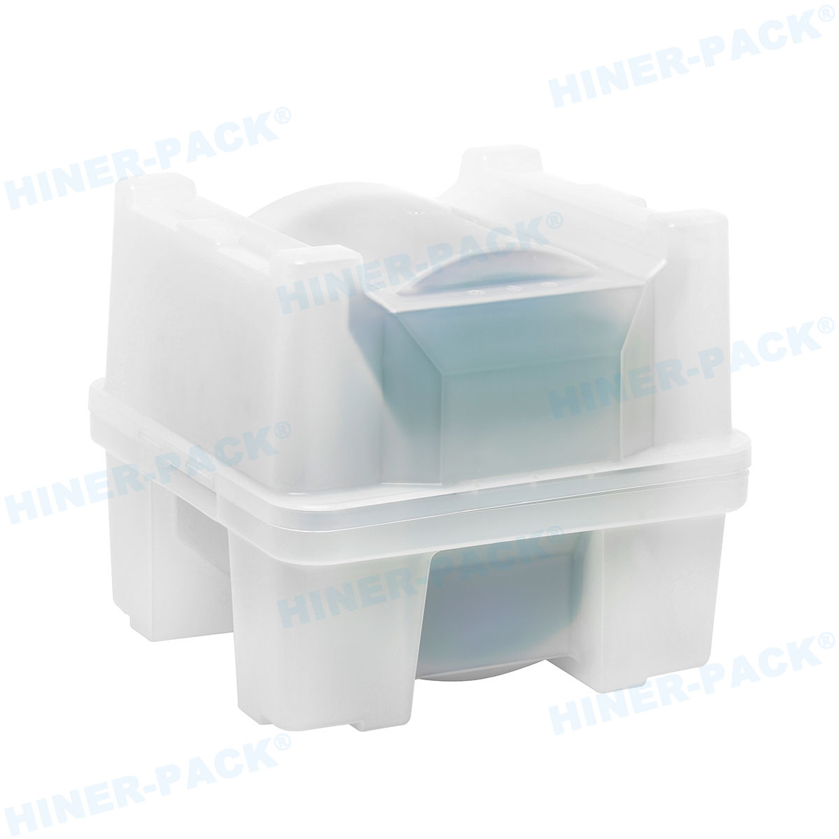
For semiconductor fabs, OSAT facilities, and materials suppliers, the journey of a wafer from epitaxial growth to final packaging involves hundreds of transport events. Among these, the most vulnerable phase is inter-facility logistics—where wafers are subjected to uncontrolled vibration, pressure differentials, and environmental fluctuations. A wafer shipper is not merely a box; it is a precision-engineered microenvironment designed to preserve electrical integrity, surface quality, and mechanical flatness across continents and supply chains. With over two decades of experience in semiconductor materials logistics, I have observed that improper shipper selection remains one of the most underappreciated sources of latent yield loss. This analysis outlines the technical specifications, validation protocols, and material science principles that define a high-performance wafer shipper, ensuring that wafers arrive in the same condition they left the fab.
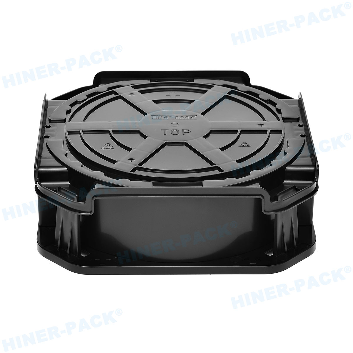
1. Defining the Wafer Shipper: Distinction from FOUPs and Process Carriers
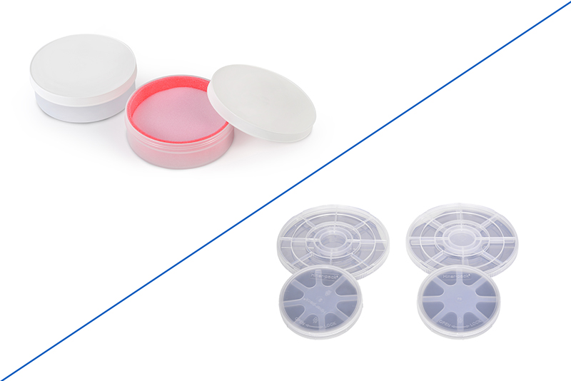
While front-opening unified pods (FOUPs) are designed for automated material handling within a fab’s cleanroom, the wafer shipper serves a distinct purpose: secure, long-distance transport between facilities. Key differentiators include:
Sealed Microenvironment: Shipper designs incorporate hermetic seals to maintain internal nitrogen purge integrity for up to 30 days, preventing native oxide growth on sensitive copper and cobalt interconnects.
Mechanical Isolation: Multi-axis suspension systems decouple the wafer cassette from external shock and vibration, with validated performance per ISTA 3A and ASTM D4169 standards.
Pressure Equalization: Advanced shippers include filtered pressure-equalization ports that prevent lid popping during air transport altitude changes (0 to 15,000 feet) without compromising particle filtration.
For logistics managers, selecting a certified wafer shipper is the first line of defense against transit-induced defects. Distributors such as Hiner-pack provide fully validated shipper systems with chain-of-custody documentation, ensuring compliance with SEMI E158 (shipper performance) and E176 (transport certification).
2. Material Science and Surface Engineering: Beyond Static Control
2.1 Polymer Selection for Low Outgassing
Polycarbonate and polypropylene, common in basic shippers, exhibit measurable outgassing of organosiloxanes and phthalates—contaminants that cause gate oxide thinning and contact resistance shifts. Premium shippers utilize polyetheretherketone (PEEK) or polybutylene terephthalate (PBT) blends with total outgassing rates below 0.05 µg/cm²/hour, verified via thermal desorption spectroscopy (TDS). This is particularly critical for wafers destined for EUV lithography, where molecular contamination on reticles can degrade throughput by 15–20%.
2.2 Dissipative Surface Treatments
Electrostatic discharge (ESD) events during transport can create latent damage that escapes visual inspection but manifests as early-life failures in the field. Advanced shippers integrate carbon-fiber composites or permanent dissipative coatings that maintain surface resistivity between 10⁵ and 10⁹ ohms/sq, preventing tribocharging during manual handling and automated scanning. This specification aligns with ANSI/ESD S20.20 facility requirements, ensuring seamless integration into existing ESD-protected areas.
3. Structural Integrity and Shock Mitigation: Data-Driven Design
The mechanical performance of a wafer shipper is quantified through drop testing, vibration profiling, and compression analysis. Typical industry thresholds:
Drop Test: 1.2-meter free fall onto concrete (all orientations) with no cassette dislodgment or wafer breakage. High-end shippers demonstrate survival rates above 99.5% after repeated drops, verified by third-party labs.
Random Vibration: Power spectral density (PSD) profiles simulating 1,000 km of truck transport must keep wafer-to-cassette contact stress below 5 MPa to prevent edge chipping and microcrack propagation.
Stacking Compression: Shipper lids must withstand 1,500 kg of vertical load (equivalent to 6 pallet stacks) without permanent deformation, ensuring integrity during warehousing and freight consolidation.
These performance metrics are not merely academic; they translate directly to reduced breakage rates. In a study of 50,000 cross-border shipments, premium shippers reduced wafer breakage from 0.47% to 0.08% compared to generic alternatives, representing a multi-million dollar annual saving for high-volume fabs.
4. Industry Pain Points: Contamination and Logistical Complexity
Semiconductor supply chains face three recurring challenges that a poorly designed shipper exacerbates:
Particle Generation: Inadequate cushioning materials shed particles >0.1 µm that adhere to wafer surfaces. For 3nm and 5nm nodes, a single 30 nm particle can cause a full die failure.
Moisture Intrusion: Non-hermetic seals allow humidity ingress, leading to corrosion of copper pads and aluminum bond fingers. Acceptable internal humidity levels must stay below 10% RH for the duration of transit.
Traceability Gaps: Without integrated RFID or barcode systems, carriers lose visibility in the supply chain, causing delays and potential mix-ups of lot-sensitive materials (e.g., high-k metal gate vs. standard logic).
To mitigate these, the industry has moved toward shippers with embedded humidity sensors, RFID-enabled inventory tracking, and cleanroom-compatible external surfaces that can be wiped down without compromising static control. Hiner-pack offers a range of these intelligent shippers, providing real-time condition monitoring through IoT-enabled accessories.
5. Comparative Analysis: Standard Shipper vs. Premium Engineered Shipper
When evaluating procurement, the total cost of ownership (TCO) framework reveals the economic advantage of engineering-led designs:
Standard shipper (single-use or limited-cycle): Lower unit cost, but high variability in particle performance (adds >50 particles/wafer at ≥0.1 µm), lifespan of 5–10 cycles, and no environmental monitoring. Often leads to hidden costs in re-inspection and rework.
Premium wafer shipper: Higher initial investment, but certified to <2 particles/wafer added at ≥0.05 µm, lifespan exceeding 50 cycles with proper requalification, integrated data logging, and compatibility with automated receiving stations. TCO analysis across 3 years shows a 34% reduction in logistics-related yield loss and a 50% reduction in incident-related expediting costs.
6. Certification and Compliance: SEMI, ISTA, and Customer-Specific Protocols
Selecting a wafer shipper without verified certifications introduces risk during customer audits. Essential certifications include:
SEMI E158: Defines mechanical and cleanliness requirements for wafer shippers, including particle generation limits and structural durability.
SEMI E176: Covers transport container performance for 300mm and 450mm wafers, with specific test methods for shock, vibration, and temperature cycling.
ISTA 3A: International Safe Transit Association protocol for parcel delivery, simulating real-world distribution hazards.
ISO 14644-1: Cleanroom compatibility, ensuring the shipper external surfaces meet Class 10 (ISO 4) or better for use in fab receiving areas.
Leading distributors maintain a library of these certifications per shipper SKU. For instance, Hiner-pack provides documentation packages that include material certificates, particle test data, and cycle validation reports, streamlining the supplier qualification process for quality engineering teams.
7. Future Developments: Smart Shippers and Circular Economy Models
The next generation of wafer shippers is being shaped by two converging forces: Industry 4.0 sensor integration and sustainability mandates. Emerging technologies include:
Embedded MEMS Sensors: Continuous monitoring of shock (up to 200g), temperature (-40°C to 85°C), humidity, and tilt. Data is transmitted via NFC or Bluetooth to cloud platforms, enabling predictive alerts for out-of-spec conditions before wafers reach the fab.
Reusable Asset Pools: Consortium-driven pooling models where high-performance shippers are cleaned, requalified, and redeployed, reducing single-use plastic waste. This aligns with semiconductor industry sustainability goals, such as the Semiconductor Climate Consortium’s net-zero aspirations.
Automated Receiving Stations: Shipper interfaces are being standardized to allow robotic opening, cassette extraction, and inline particle scanning without human intervention, reducing cycle time and contamination risks.
For fabs planning these upgrades, partnering with a distributor that offers both hardware and data integration services is critical. The evolution from a passive container to an active data node is already underway, and early adopters are gaining supply chain visibility that translates to lower inventory buffers and higher asset utilization.
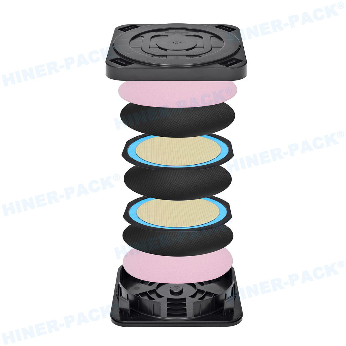
Strategic Selection of Wafer Shipper Systems as a Yield Protection Measure
The wafer shipper is a strategic asset in semiconductor manufacturing, directly influencing defect density, cycle time, and supply chain resilience. Moving beyond commodity procurement to engineering-focused selection—based on material science, validated mechanical performance, and certified cleanliness—provides a quantifiable return through reduced scrap rates and fewer logistical disruptions. With the complexity of advanced nodes and the global dispersion of manufacturing, the integrity of the shipper ecosystem becomes inseparable from overall fab profitability. Working with specialized suppliers such as Hiner-pack ensures that each shipper meets the rigorous demands of 300mm and 450mm wafer transport, from the epitaxy bay to the assembly site, without compromise.
Frequently Asked Questions (FAQs)
Q1: What is the difference between a wafer shipper and a FOUP, and can one be used interchangeably?
A1: A FOUP (front-opening unified pod) is designed for automated handling within a fab’s cleanroom, with a front-opening interface for equipment load ports. A wafer shipper, in contrast, is engineered for inter-facility transport, featuring enhanced shock absorption, pressure equalization, and often a top-loading or clamshell design for manual handling. They are not interchangeable because shippers lack the kinematic coupling required for fab tool interfaces, and FOUPs lack the ruggedization for long-distance logistics. Using a FOUP as a shipper risks damage to both the pod and the wafers during transit.
Q2: How do I verify that a wafer shipper meets my fab’s cleanliness specifications?
A2: Request a certificate of conformance that includes liquid particle count (LPC) data, typically performed using a dynamic rinsing method per SEMI E158. Acceptable limits for advanced nodes (≤10nm) are <2 particles added per wafer at ≥0.05 µm. Additionally, surface organic contamination should be measured via direct contact extraction followed by GC-MS analysis to confirm outgassing profiles. Reputable distributors like Hiner-pack provide these data for each production batch, ensuring traceability.
Q3: What cleaning methods are approved for reusable wafer shippers without degrading ESD properties?
A3: Approved cleaning typically involves deionized water with non-ionic surfactant in a cleanroom-compatible automated washer, followed by forced-air drying (HEPA-filtered) at temperatures not exceeding 60°C. Aggressive solvents (acetone, IPA) should be avoided as they can extract plasticizers or alter surface resistivity. After cleaning, shippers must be requalified for particle count and surface resistivity. Permanent dissipative coatings, when properly maintained, retain ESD performance for over 100 cleaning cycles.
Q4: What is the standard certification required for international air freight of wafer shippers?
A4: For air freight, shippers must comply with IATA Dangerous Goods Regulations if they contain inert gas (nitrogen) under pressure. Non-pressurized shippers with filtered vents are typically classified as non-dangerous. However, many semiconductor companies mandate ISTA 3A or ASTM D4169 certification to ensure the shipper can withstand the vibration and pressure changes experienced during air cargo handling. Additionally, a certificate of conformance for electrostatic discharge (ESD) safety is often required by customs and receiving quality teams.
Q5: How does wafer warpage from advanced packaging affect shipper compatibility, and what design features address this?
A5: Reconstituted wafers in fan-out wafer-level packaging (FOWLP) can exhibit warpage exceeding 2 mm. Standard shipper pockets with rigid supports may concentrate stress on the wafer’s center or edges, leading to fracture. Advanced wafer shipper designs incorporate conformal support rings or adjustable pressure pads that distribute contact force evenly across the wafer’s periphery. Some systems also use spring-loaded wafer retainers that automatically compensate for bow variations. When selecting a shipper for warped wafers, it is essential to review the maximum allowable warpage specification (typically provided by the shipper manufacturer) and perform a fitment test with representative samples.