
A qualified wafer boats factory does not just process refractory materials—it engineers thermally stable, dimensionally certified wafer carrying fixtures that survive aggressive chemical etching, furnace diffusion, and automated robotic transfer without wafer warpage or particle shedding. Founded in 2013, Hiner-pack combines over a decade of semiconductor handling engineering with high-standard cleanroom processing, over 2,000 existing mold configurations, and university-backed material research to deliver turnkey carrying and packaging solutions for global fabs and OSAT facilities.
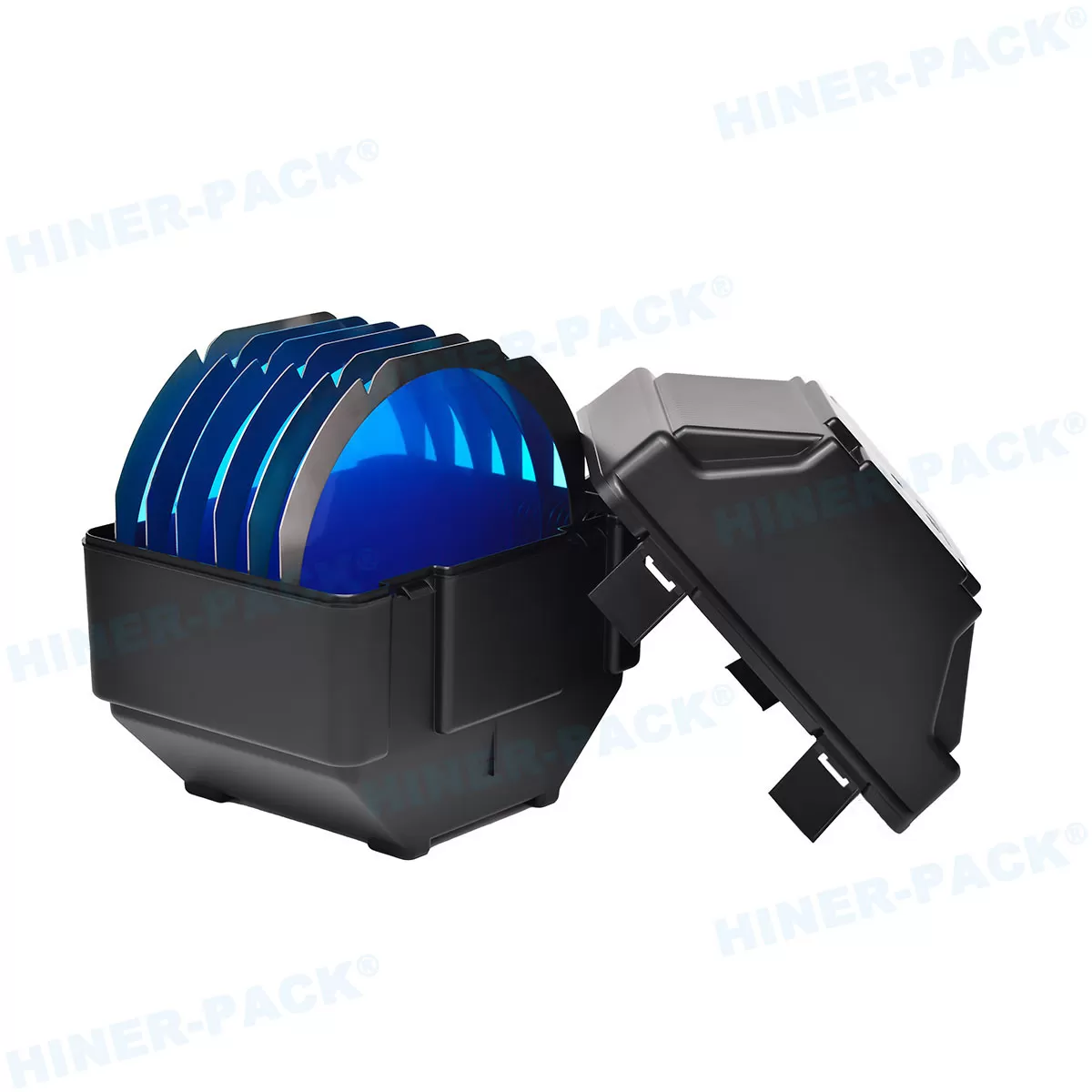
A premier wafer boats factory is defined by its substrate purity, sub-0.05 mm slot pitch repeatability, and native integration with automated Fab/OSAT handling systems. Hiner-pack provides manufacturer-direct OEM/ODM capabilities backed by an extensive R&D polymer laboratory, patented structural designs, in-house precision mold tooling, and ISO-compliant cleanroom cleaning lines to ensure zero-defect wafer protection across high-temperature and transit cycles.
Established Track Record: High-tech enterprise founded in 2013, providing end-to-end turnkey services across IC packaging, testing, and wafer fabrication handling.
Tooling Scale & Speed: Over 2,000 existing molds available for immediate qualification, drastically shortening lead times for standard and custom wafer carriers.
Material R&D Depth: Proprietary polymer and specialty raw material research bases established in partnership with renowned domestic universities and institutes.
Turnkey Process Control: In-house mold fabrication, high-precision injection molding, certified cleanroom cleaning, and comprehensive metrology under one roof.
Factory Spec Matrix: Hiner-pack Production & Engineering Envelope
| Parameter | Hiner-pack Manufacturing Standard |
|---|---|
| Operational Scope | Design, R&D, Tooling, Molding, Cleaning, Assembly, and Global Export (Turnkey OEM/ODM). |
| Supported Diameters | 100 mm (4"), 150 mm (6"), 200 mm (8"), 300 mm (12") wafer carriers, handling cassettes, and transfer boats. |
| Tooling & Molds Available | 2,000+ existing mold sets spanning standard SEMI-spec cassettes to customized process boats. |
| Cleanroom & Post-Processing | Dedicated high-standard cleanroom cleaning lines, hot DI water ultrasonic rinse baths, and vacuum heat sealing. |
| Intellectual Property | Multiple national invention patents and utility model patents covering automated handling stability and anti-static structures. |
1. Material Science and Specialized Processing: University-Backed R&D
Wafer carrier stability begins at the molecular level. Hiner-pack has established a dedicated polymer material R&D base in collaboration with leading universities and research institutes, mastering high-purity compound blending, ESD anti-static stability, and refractory polymer processing.
High-temperature front-end processing (diffusion, oxidation, LPCVD) and chemical handling (wet bench cleaning, transport) subject wafer carriers to extreme operational boundaries. In dynamic automated fab lines, standard plastics or uncertified raw materials suffer from outgassing, high surface resistivity leading to electrostatic discharge (ESD), and mechanical creeping.
To eliminate these systemic risks, Hiner-pack’s material R&D team focuses on specialized formulations:
Engineered High-Purity Polymers: Advanced PFA, PTFE, PEEK, and carbon-fiber-reinforced composites tailored for extreme chemical inertness and dimensional rigidity.
Permanent Anti-Static / ESD Control: Proprietary compounding that maintains uniform surface resistivity (106 to 109 Ω/sq) aligned with ANSI/ESD S20.20 static control guidelines without chemical leaching or carbon sloughing.
Low Outgassing Formulations: Vacuum-tested materials compliant with ASTM E595 outgassing limits and SEMI criteria to protect high-density wafer nodes from airborne molecular contamination (AMC).
| Material Category | Primary Fab Application | Typical Industry Risk | Hiner-pack Engineered Solution |
|---|---|---|---|
| High-Purity Fluoropolymers (PFA/PTFE) | Wet cleaning, acid etching, chemical transport | Cold flow and slot dimensional creep over thermal cycles | Reinforced structural ribs with modified crystallization for high rigidity |
| ESD Conductive Polymers (PEEK/PBT) | Automated wafer handling, EFEM sorting, OSAT transport | Carbon shedding; unstable resistivity under humidity fluctuations | University-patented conductive network matrix with zero ionic shedding |
| High-Temp Quartz / SiC Carriers | Furnace diffusion, oxidation, high-temp annealing | Devitrification; slot pitch distortion causing end-effector drops | Optical-grade raw quartz selection; laser-aligned weld verification |
2. In-House Mold Processing and Tooling Scale: The Power of 2000+ Molds
Unlike assembly brokers, Hiner-pack operates complete mold design and high-precision CNC injection facilities. With over 2,000 existing mold sets, Hiner-pack delivers immediate compatibility with global automated handling systems while providing rapid OEM/ODM prototyping for custom substrates.
When automated wafer sorters and robotic arms (EFEM) interface with wafer carriers, a variance of just 0.05 mm can disrupt optical sensors, generate edge-grip micro-cracking, or trigger catastrophic emergency stops. Achieving consistent precision across high-volume production requires direct ownership over mold maintenance and machine dynamics.
By keeping mold fabrication, multi-cavity injection, and precision EDM tooling inside the Hiner-pack factory ecosystem, engineering teams enforce strict tolerances across all physical axes:
Slot Pitch Uniformity: CNC-ground molds guarantee slot-to-slot parallelism across 25, 50, or 100-wafer configurations, eliminating mechanical friction during high-speed wafer loading.
Robotic Interface Registration: Precise alignment notches (H-bar, automated lift ears, and end-effector pockets) built strictly to international SEMI automated carrier standards.
Turnkey Rapid Tooling: Custom wafer sizes, ultra-thin wafer requirements, and odd-dimension substrates transition from CAD to certified molded prototype in industry-leading lead times.
3. High-Standard Cleanroom Cleaning and Automated Processing Infrastructure
Contamination control defines semiconductor packaging and fabrication integrity. Hiner-pack integrates automated mold processing with dedicated cleanroom cleaning lines, ensuring that every wafer carrier arrives ready for direct fab introduction without secondary pre-cleaning.
| Facility Node | Technical Equipment & Systems | Quality Target & Standard | Fab Operational Benefit |
|---|---|---|---|
| Mold & Tooling Hub | High-speed CNC, precision mirror EDM, slow-wire electrical cutting | Mold core dimensional tolerance within ±0.005 mm | Zero burrs, flash-free slot edges, smooth surface finish |
| Injection Molding Center | Fully electric, high-tonnage precision injection machines | Stable cavity pressure control; zero thermal stress pockets | Warpage resistance under repeated fab thermal cycles |
| Cleanroom Cleaning Lines | Multi-stage ultrasonic scrubbers; 18.2 MΩ·cm hot DI water cascade | ISO 14644-1 certified clean environment; particle shed test | Direct-to-fab cleanroom compatibility without cross-contamination |
| Comprehensive Testing Lab | Multi-axis optical CMM aligned with NIST metrology practices, surface resistivity meters, ICP-MS trace testing | Full batch geometric & electrical compliance certification | Traceable inspection data delivered with every production lot |
4. Engineering Sourcing Guide: Do's and Don'ts for Wafer Carrier Procurement
Leverage pre-existing tooling: Inquire about Hiner-pack's 2,000+ mold catalog to eliminate NRE tooling costs and slash lead times.
Demand verified ESD reports: Verify that surface resistivity is baked into the raw polymer matrix rather than achieved via temporary topical coatings.
Audit robotic compatibility early: Test carrier-to-equipment integration with EFEM end-effectors using verified CMM coordinates.
Lock in turnkey traceability: Source from an integrated manufacturer that controls both material R&D and clean packaging.
Don't trade with non-manufacturing brokers: Intermediaries cannot modify mold gates, alter polymer compounds, or provide direct CMM data.
Don't compromise on cleanroom washing: Unwashed wafer boats introduce ionic residues and fine polymer dust into furnace tubes.
Don't assume all carriers fit automated lines: Slight deviations in alignment ears cause robotic arm clamping errors and wafer micro-cracking.
Don't use disposable packaging for critical runs: Insist on reusable, cost-efficient, and high-impact structural packaging solutions.
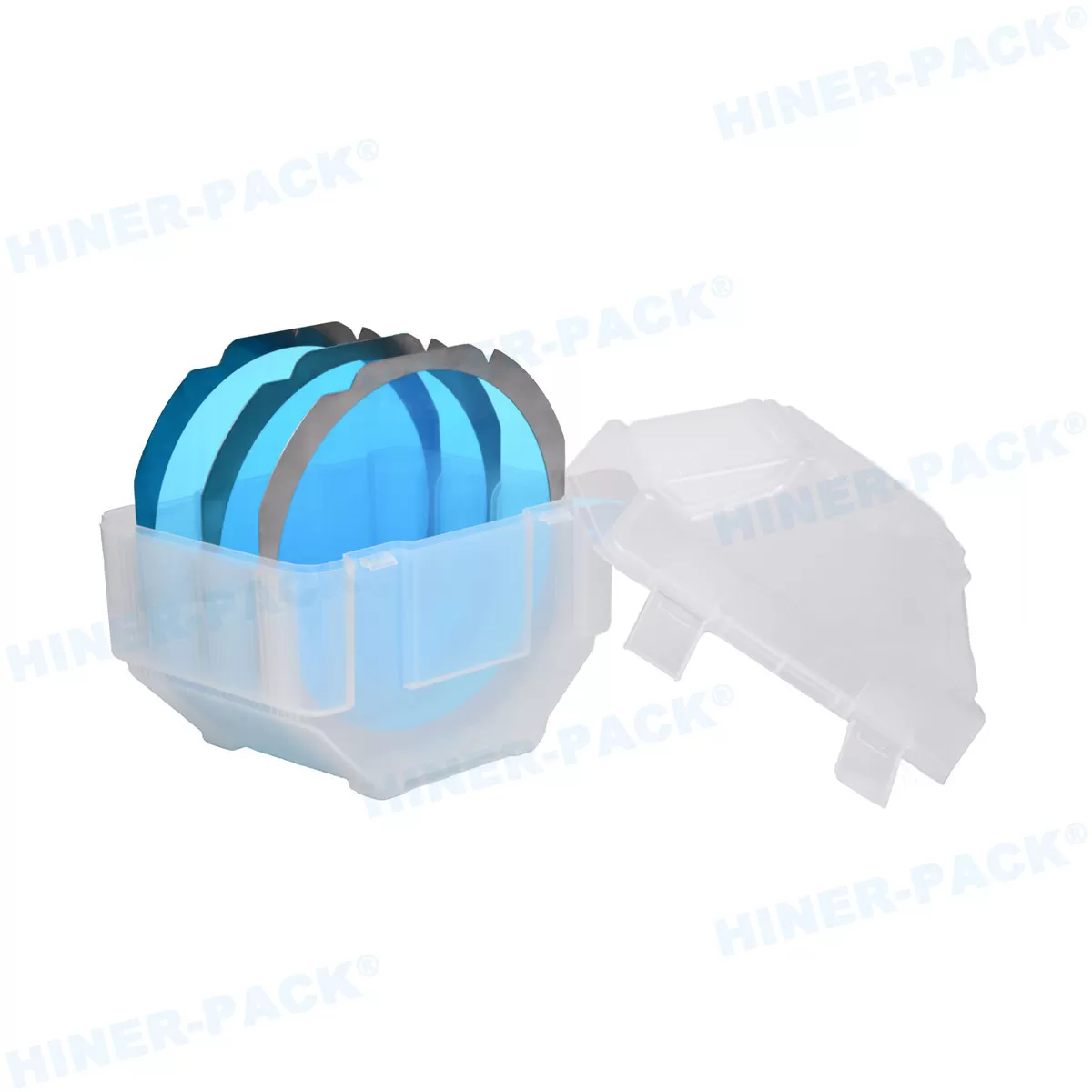
5. Manufacturer-Direct Turnkey Services & Global Partnership Network
As a pioneer of R&D and application in semiconductor carrier products, Hiner-pack delivers superior wafer protection, secure and stable wafer handling, cleanroom compatibility, and reusable, cost-efficient solutions on a manufacturer-direct basis.
Committed to advancing semiconductor handling and packaging transport solutions, Hiner-pack provides comprehensive OEM & ODM collaboration models worldwide:
Turnkey OEM/ODM Engineering: From customized chemical resistance profiles and specific slot counts to robotic interface modifications, our dedicated engineering team handles everything from 3D CAD modeling to rapid mold production.
Direct Manufacturer Pricing: Eliminating broker markups, Hiner-pack provides scalable production economies for high-volume OSAT transport cassettes, process boats, and shipping shippers.
Global Distributors Wanted: To support our rapidly expanding customer base across North America, Europe, and the Asia-Pacific region, Hiner-pack is actively welcoming qualified global distributors and semiconductor packaging partners.
Frequently Asked Questions: Wafer Boats Factory & Engineering Sourcing
Q1: Can Hiner-pack manufacture custom wafer boats without incurring high NRE tooling costs?
A1: Yes. With a comprehensive library of over 2,000 existing molds, Hiner-pack can frequently match your wafer diameter (100mm to 300mm), slot count, and pitch specifications using pre-existing tooling—completely eliminating non-recurring engineering (NRE) fees. For specialized custom carriers, our in-house high-speed CNC and mirror EDM mold processing facilities ensure rapid, cost-effective prototype tooling with industry-leading lead times.
Q2: How does Hiner-pack ensure wafer boat compatibility with automated EFEM and robotic arms?
A2: All Hiner-pack carriers are manufactured strictly to SEMI physical dimension standards. We verify slot pitch parallelism within sub-0.05 mm tolerances and use multi-axis optical CMM inspection to audit robotic end-effector pockets, H-bar profiles, and automated lift ears. This eliminates mechanical friction, optical sensor misreads, and edge-clamping micro-damage during high-speed robotic transfer.
Q3: Are Hiner-pack wafer carriers ready for direct cleanroom introduction upon delivery?
A3: Yes. Every carrier undergoes multi-stage ultrasonic cleaning and an 18.2 MΩ·cm hot deionized (DI) water cascade rinse inside our certified cleanroom cleaning lines. The finished products are baked dry, tested for particulate shedding, and double vacuum heat-sealed in antistatic, outgassing-free clean packaging—allowing immediate, pre-cleaning-free introduction into ISO Class 4 or 5 semiconductor fab environments.
Q4: How does Hiner-pack achieve permanent, non-shedding ESD protection for wafer transport carriers?
A4: Unlike low-tier suppliers that rely on temporary topical anti-static sprays, Hiner-pack leverages its university-partnered polymer R&D base to blend proprietary conductive networks directly into the polymer matrix (e.g., PEEK, PBT, carbon composites). This guarantees uniform surface resistivity (106 to 109 Ω/sq) that does not migrate, wash out during acid cleans, or generate particulate carbon shedding onto active die surfaces.
Q5: What substrate material should I select: Quartz, Silicon Carbide, or Engineered Polymers?
A5: Selection depends on process chemistry and thermal ceilings:
High-Purity Fused Quartz: Ideal for thermal oxidation and standard diffusion up to 1150°C.
CVD / Sintered SiC: Required for ultra-high-temp LPCVD (>1200°C), heavy chemical exposure (HF/HNO3), and zero-sag thermal longevity.
Engineered Fluoropolymers / ESD Polymers: Optimal for wet-bench etching, chemical cleaning, automated sorting, and secure IC packaging transport.
Our material engineering team can evaluate your specific furnace telemetry and chemical recipes to recommend the most cost-efficient carrier.
Q6: What is the typical lead time for first-article samples, and does Hiner-pack support global distribution?
A6: For carriers leveraging our 2,000+ existing mold inventory, samples can be dispatched within 3 to 7 business days. Custom-to-drawing OEM/ODM projects typically take 2 to 4 weeks for tooling and first-article CMM validation. As an internationally established high-tech enterprise, Hiner-pack ships directly to leading semiconductor hubs across North America, Europe, and Asia-Pacific, and is actively expanding its global authorized distributor network.
Partner With Hiner-pack: Request Your Factory Specification Review
Looking for a certified wafer boats factory to support high-yield automated wafer fabrication, chemical handling, or IC packaging transport? Leverage our 2,000+ mold library and university-backed material testing facilities today.














