
Introduction: The Role of Substrate Protection in Semiconductor Fabrication
In modern microelectronics manufacturing, preserving substrate integrity during transport and storage is a fundamental operational requirement. Silicon wafers are highly sensitive to physical disturbances, organic outgassing, and environmental particulates. Even a microscopic contaminant can interrupt circuit pathways, leading to structural failures and lowered yield rates. Consequently, partnering with a reliable wafer carriers supplier is indispensable for fabs and packaging facilities aiming to secure their yield margins.
The transport of semiconductor substrates involves an intricate logistical path. Wafers must travel between distinct cleanroom bays, chemical processing units, and global testing facilities. During this journey, they rely entirely on containment systems to isolate them from environmental hazards. These specialized containers are designed not merely as packaging, but as active protective barriers that interact directly with the wafers and high-precision automation systems. Selecting the correct materials and engineering configurations determines the success of these protective measures.
Key Challenges in Semiconductor Substrate Logistics
To understand the design requirements of wafer packaging, one must examine the specific physical and chemical challenges that substrates encounter during distribution and internal fab routing.
Particulate Contamination
Suspended particulates in the ambient air pose a constant threat to open silicon surfaces. If particles settle on a wafer prior to photolithography or deposition, they obstruct the light path or alter film uniformity, causing structural defects. Sub-micron particulate control requires carriers to be manufactured from ultra-low-wear polymers that do not shed particles during mechanical contact or automated transfer cycles.
Electrostatic Discharge (ESD)
Insulative plastics tend to accumulate static charges via triboelectric friction during handling and transport. This static buildup introduces two primary hazards: electrostatic attraction (ESA), which pulls airborne particulates directly onto the wafer surface, and sudden electrostatic discharge (ESD), which can destroy delicate sub-micron gate oxides. A competent wafer carriers supplier must provide materials with tailored electrical properties to discharge static safely and consistently.
Chemical Outgassing
Standard industrial plastics often release volatile organic compounds (VOCs) over time, a process known as outgassing. Within a sealed wafer container, these organic molecules can condense onto the active surface of the silicon, forming an extremely thin, undesirable layer of molecular contamination. This organic film can interfere with subsequent thin-film deposition and etching processes, leading to poor adhesion or unwanted electrical resistance.
Mechanical Stress and Vibration
Road logistics, air transport, and automated material handling systems (AMHS) subject wafer containers to constant vibration and potential shock. If the structural design of the carrier does not absorb these mechanical forces, wafers can experience edge chipping, surface scratching, or complete micro-fracturing. The internal support structures, such as slots and retaining springs, must provide secure immobilization without applying localized stresses that exceed the fracture limit of the silicon crystal.
Material Engineering in Wafer Carrier Manufacturing
The choice of raw polymers is the most critical factor in mitigating the contamination and mechanical risks discussed above. Different processing stages demand specific material formulations to withstand chemical exposures, high temperatures, and static accumulation.
High-performance engineering polymers form the foundation of modern cleanroom-compatible wafer handling systems. Hiner-pack utilizes specialized polymer formulations to ensure high structural stability and low particle generation. Below are the primary materials utilized in this field:
Polyetheretherketone (PEEK): This advanced thermoplastic exhibits exceptional mechanical strength, wear resistance, and thermal stability. Carbon-fiber-reinforced PEEK is widely used for high-temperature cassette systems and automated handling components due to its structural rigidity and reliable ESD dissipation characteristics.
Polycarbonate (PC): Offering high impact resistance and dimensional stability, polycarbonate is the standard material for transparent outer enclosure shells, such as shipping boxes. It allows for optical inspections without exposing the wafers to the open atmosphere, while maintaining excellent physical protection.
Fluoropolymers (PFA/PTFE): Extremely inert and highly resistant to aggressive acids and solvents, fluoropolymers are used in wet-processing cassettes where chemical exposure is intense. However, because they are softer than PEEK or Polycarbonate, they require precise manufacturing to prevent dimensional distortion under load.
Modified Polypropylene (PP): Often chosen for intermediate storage and cost-efficient shipping options, modified polypropylene provides a balanced mix of flexibility and chemical resistance, provided it is treated with anti-static agents to control charge accumulation.
Process Criteria for Selecting a Wafer Carriers Supplier
Evaluating a potential wafer carriers supplier requires a systematic review of their engineering capabilities, cleanroom compliance, and quality control systems.
Compliance with SEMI Standards
The semiconductor industry relies heavily on automation. Front Opening Unified Pods (FOUPs), cassettes, and automated shippers must comply precisely with SEMI (Semiconductor Equipment and Materials International) standards, such as SEMI M1, SEMI E1.9, and SEMI E111. These specifications define the dimensions, pocket configurations, and automated interface points required for robot grippers and fab tool loadports. A supplier must demonstrate that their tooling and molding processes maintain tolerances within fractions of a millimeter to prevent automated handling errors.
Cleanroom Production Environments
Because the carrier is designed to protect wafers from contamination, the carrier itself must be manufactured in an environment that limits particulate introduction. Precision injection molding, assembly, and packaging should ideally occur within ISO Class 4 or Class 5 cleanroom conditions. Any residual particulate matter from the molding process must be eliminated through automated washing cycles using multi-stage deionized water systems before the products are double-bagged for delivery.
Traceability and Material Consistency
Semiconductor manufacturing is sensitive to even minor changes in material chemistry. A qualified supplier must offer complete batch traceability for every run of polymer resin. Any change in the polymer supplier, masterbatch formulation, or colorant additives can alter the outgassing profile or static dissipative performance of the finished container, potentially disrupting the customer’s production yield.
Customization and Specialized Container Configurations
Not all semiconductor components fit into standard, high-volume production categories. Smaller R&D facilities, compound semiconductor foundries (working with Gallium Nitride or Silicon Carbide), and specialized packaging houses require tailored handling solutions.
As a manufacturing specialist, Hiner-pack designs custom containment options that cater to distinct processing scenarios, ensuring that unique wafer sizes and fragile compound materials are fully protected. Below are the typical product configurations available:
Single-Wafer Shippers (Coin-Style): Ideal for low-volume distribution, research prototypes, or high-value compound semiconductor wafers. These containers use internal elastomeric cushions or precise retention rings to immobilize a single substrate, preventing any contact with the active face of the wafer.
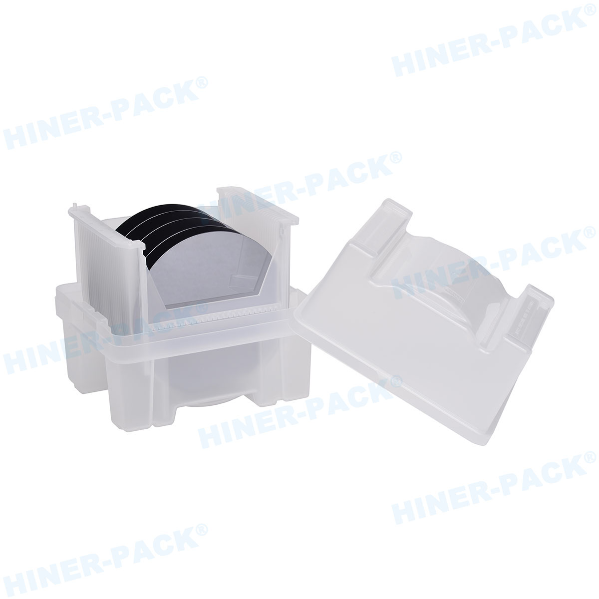
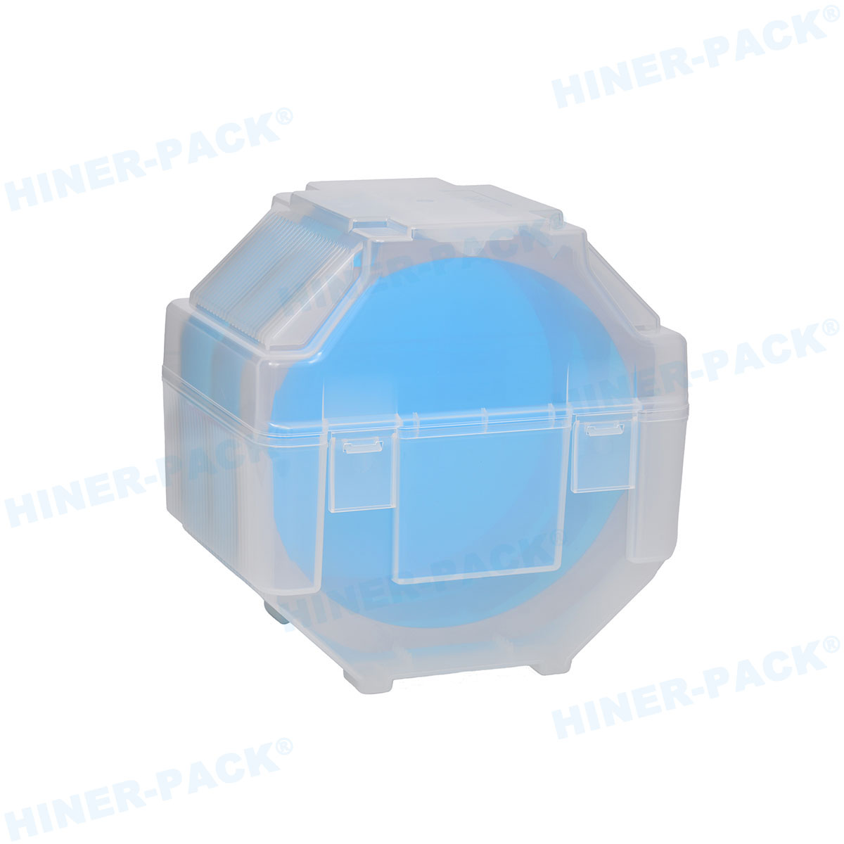
Multi-Wafer Shipping Boxes: Designed for bulk logistics, these boxes hold 25 wafers securely. They often feature an internal cassette or shell combination, supported by external shock-absorbing structures, to minimize the transmission of vibrational energy during international shipping.
Process Cassettes: Open-structure carriers designed to hold wafers during chemical cleaning, photolithography, or thermal processing. These cassettes feature wide slot spacing to maximize fluid dynamics or airflow, ensuring uniform chemical contact and rapid drying.
In-Process Storage Boxes: Sturdy, dust-tight boxes used to store wafers between processing steps within the cleanroom, protecting them from localized airflow turbulence and transient electrostatic charges.
Quality Testing Protocols for Wafer Shippers
A reputable wafer carriers supplier must implement rigorous verification protocols to ensure every batch meets the demanding requirements of the semiconductor industry. These testing protocols should include:
| Test Category | Testing Method | Operational Purpose |
|---|---|---|
| ESD Verification | Surface Resistivity Measurement (Ohms/Sq) | Confirms that dissipative materials remain within the safe range of 105 to 109 ohms/sq, preventing rapid static discharges. |
| Outgassing Analysis | Gas Chromatography-Mass Spectrometry (GC-MS) | Identifies volatile organic contaminants to ensure the plastic does not release harmful molecular compounds onto wafer surfaces. |
| Dimensional Metrology | Coordinate Measuring Machines (CMM) and Optical Scanning | Verifies compliance with SEMI standards to prevent jam-ups or registration errors in automated fab loadports. |
| Mechanical Durability | Simulated Drop and Vibration Profile Testing | Evaluates the shock-absorption capabilities of the shippers to protect wafers against real-world logistical impacts. |
| Particulate Cleanness | Liquid Particle Counting (LPC) | Measures the concentration of residual surface particles on the carriers after the cleanroom washing process. |
Securing Your Semiconductor Supply Chain
In a market where microchip production schedules operate on tight deadlines, wafer damage or delivery delays can result in severe operational setbacks. Establishing a long-term partnership with a dedicated wafer carriers supplier is a strategic step toward ensuring supply chain resilience. By working with a manufacturer that controls the entire production cycle—from raw polymer compounding and cleanroom molding to final optical inspection—semiconductor fabs can secure consistent, high-yield results. Hiner-pack maintains extensive cleanroom production facilities and material reserves to support fluctuating global wafer transport demands, providing continuous product availability and reliability.
Inquire Now for Reliable Wafer Protection Solutions
Protecting high-value silicon substrates requires precision engineering and reliable cleanroom-compatible materials. If your facility is planning a transition to automated material handling systems, facing yield losses due to ESD or particulate contamination, or searching for customized carrier sizes, our engineering team is ready to assist. Please contact us to discuss your design requirements, request material safety data sheets, or obtain physical samples for cleanroom evaluation. Submit your inquiry today and secure your substrate logistics.
Frequently Asked Questions (FAQ)
Q1: What is the main difference between ESD conductive and ESD dissipative wafer carriers?
A1: ESD conductive materials have a lower electrical resistance (typically under 105 ohms/sq) and allow static charges to flow rapidly across the surface. ESD dissipative materials have a higher, controlled resistance (typically between 105 and 109 ohms/sq), which slows down the discharge rate. In semiconductor manufacturing, dissipative materials are generally preferred for wafer-contact components because they discharge static gently, minimizing the risk of localized damage to delicate micro-circuits.
Q2: How does polymer outgassing impact silicon wafers during long-distance shipping?
A2: During long shipping cycles, temperature variations can cause plastic carriers to release volatile organic compounds (VOCs). If these gases accumulate inside a sealed container, they condense on the highly reactive surface of the silicon wafers. This organic film can interfere with subsequent process steps, such as wafer bonding, etching, or thin-film deposition, resulting in poor adhesion or erratic electrical behavior.
Q3: Why are SEMI standards so important for wafer carriers?
A3: SEMI standards establish universal dimensional guidelines for the semiconductor industry. Since modern fabrication facilities rely heavily on automated material handling systems, robot end-effectors, and tool loadports, any minor variation in carrier dimensions could cause mechanical jams, dropped wafers, or sensor errors. Compliance with SEMI standards ensures that carriers interface correctly with equipment from different manufacturers worldwide.
Q4: Can wafer shipping boxes be cleaned and reused, or are they single-use items?
A4: Many wafer shipping boxes are structurally durable enough for multiple cycles. However, reuse requires a strict cleanroom washing protocol. Over time, polymers can accumulate static charges, particulate buildup, and microscopic scratches that trap contaminants. Fabs must verify the cleanroom compatibility and surface resistivity of reused containers before introducing them back into the production cycle, while some high-reliability applications mandate single-use configurations.
Q5: What sizes of wafers can be accommodated by standard carrier configurations?
A5: Standard configurations support wafer diameters ranging from 100mm (4-inch), 150mm (6-inch), 200mm (8-inch), to 300mm (12-inch). For specialized compound semiconductors, optical substrates, or research applications, manufacturers also provide custom-designed carriers for smaller sizes like 2-inch or 3-inch wafers, as well as customized pocket designs for non-standard wafer thicknesses.














