
In the semiconductor manufacturing process, the journey from raw silicon ingot to a finished integrated circuit is filled with physical and chemical hazards. As fabrication facilities push the limits of physics with sub-3nm process nodes, even sub-micron particulate contamination or microscopic structural deviations can lead to devastating yield losses. Wafers must be transported between exposure steps, etching baths, metrology stations, and packaging facilities with absolute stability and cleanliness.
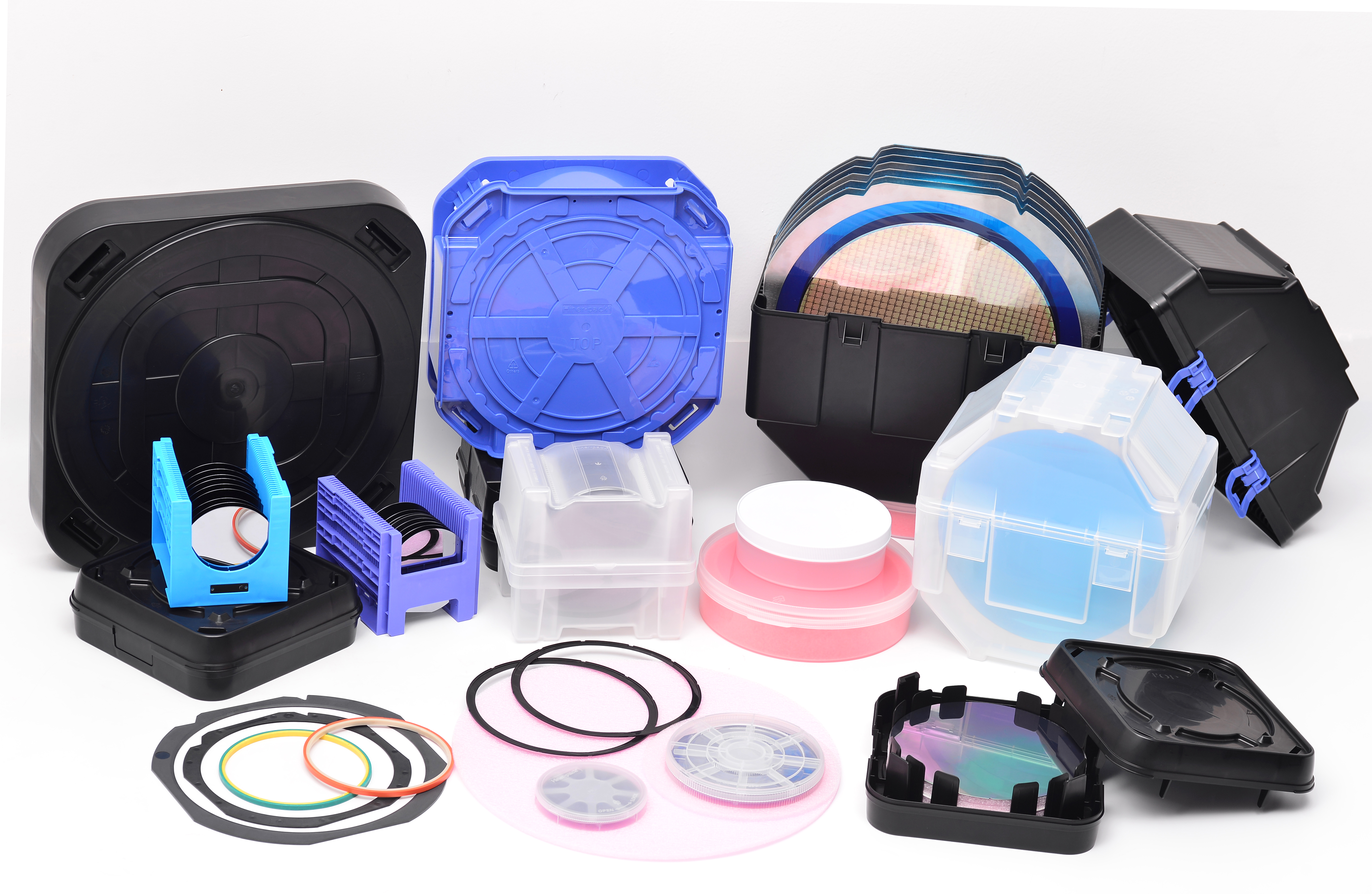
At the center of this secure transport system are wafer carriers. These specialized enclosures and cassettes must provide structural protection, prevent physical degradation, and withstand aggressive chemicals and high temperatures. For cleanroom engineers and procurement professionals, partnering with a qualified wafer carriers manufacturer is a decisive step in maintaining wafer integrity and securing the entire fabrication loop.
1. Polymer Science in Wafer Carrier Construction
The performance of a wafer carrier is deeply connected to the polymer compound from which it is molded. Standard plastics do not suffice in high-vacuum, high-temperature, or chemically aggressive environments. Semiconductor fabs require highly engineered polymers with distinct structural and chemical properties.
High-Performance Fluoropolymers and Engineering Plastics
Polyetheretherketone (PEEK): Known for outstanding mechanical strength and dimensional stability at high temperatures, PEEK is the material of choice for demanding automated handling environments. It exhibits exceptionally low wear rates and minimal outgassing under high vacuum conditions, preventing structural sagging during thermal cycles.
Perfluoroalkoxy (PFA): Renowned for its near-total chemical inertness, PFA is widely utilized in wet processing applications. It resists corrosion from strong acids, bases, and organic solvents, ensuring that carriers do not degrade or leach metallic ions into chemical baths.
Polycarbonate (PC) and Polypropylene (PP): Typically selected for shipping containers and low-temperature storage cassettes, these materials provide reliable impact resistance and cost-effective physical protection during transport outside the primary cleanroom loop.
Electrostatic Discharge (ESD) Mitigation
Pure polymers are inherently electrical insulators, making them prone to accumulating static charges. In a cleanroom, electrostatic attraction (ESA) pulls airborne molecular contaminants directly onto the wafer surfaces. Furthermore, an uncontrolled electrostatic discharge (ESD) event can destroy delicate circuitry on active wafers.
To prevent this, specialized manufacturers like Hiner-pack integrate conductive additives, such as carbon fibers or carbon nanotubes, into the polymer matrix. This engineering adjustment lowers the surface resistivity to the dissipative range (typically 105 to 109 ohms per square), allowing static charges to flow safely to ground without shedding conductive carbon particles that could cause particulate contamination.
2. Geometric Precision and Automated Material Handling Systems (AMHS)
Modern semiconductor fabs operate with high levels of automation. Overhead Hoist Transport (OHT) systems, Automated Guided Vehicles (AGVs), and robotic end-effectors continuously move wafers from one tool to another. This automation leaves no room for dimensional variations.
Compliance with SEMI Standards
A high-quality carrier must comply strictly with SEMI (Semiconductor Equipment and Materials International) standards. These regulations govern every key dimension of the carrier, including kinematic coupling pin placement, door latch mechanisms, and carrier robotic flanges. Minor structural warpage or deviations in slot pitch can cause robotic misalignments, leading to handling errors, wafer sliding, or catastrophic breakage inside automated process tools.
Slot Design and Structural Parallelism
The internal slots of a wafer cassette must be engineered with high precision. Parallelism between slots must be maintained across the entire height of the carrier to ensure uniform spacing. This uniform spacing is necessary to:
Prevent adjacent wafers from contacting each other during transport vibrations.
Optimize the flow of inert purging gases, such as nitrogen, within Front Opening Unified Pods (FOUPs) to maintain low relative humidity levels.
Facilitate smooth insertion and extraction by robotic vacuum wands without scraping the wafer edges, which can generate microscopic silicon dust.
3. Criteria for Selecting a wafer carriers manufacturer
When evaluating suppliers for wafer handling equipment, procurement and engineering teams must look beyond basic manufacturing capabilities. The production of these high-performance carriers requires specialized facilities and rigorous quality control protocols.
Cleanroom Production and Injection Molding Excellence
High-precision carriers must be molded and assembled in certified ISO Class 4 or Class 5 cleanroom environments. Any microscopic dust particle present in the molding room can become embedded within the polymer structure during injection, later creating a contamination hazard during fab operations. An experienced wafer carriers manufacturer must maintain stringent cleanroom standards and use specialized low-residue mold release agents to guarantee high purity.
Metrology and Validation Capabilities
A reliable supplier must prove dimensional compliance using coordinate measuring machines (CMM) and optical scanning systems. Thermal cycling chambers are also required to verify that the carriers maintain their exact dimensions after repeated exposure to elevated temperatures. Additionally, outgassing tests must be conducted periodically using gas chromatography-mass spectrometry (GC-MS) to ensure that volatile compounds remain below the parts-per-billion (ppb) threshold.
4. Special Considerations for Compound Semiconductors and Thin Wafers
The growth of high-power electronics, RF systems, and advanced packaging has introduced new substrates to the fabrication floor, including Silicon Carbide (SiC), Gallium Nitride (GaN), and ultra-thin silicon wafers used in 3D-stacked architectures.
Handling High-Density and Brittle Substrates
SiC and GaN wafers are significantly denser and more brittle than standard silicon. Their higher weight increases the physical load on the cassette slots, requiring reinforced rib structures to prevent structural sagging. Additionally, because these substrates are highly valuable, physical protection during transport is paramount. Custom pocket designs and shock-absorbing elastomeric retention systems are deployed to protect these brittle wafers from microscopic edge-chipping.
The Challenge of Thin Wafer Warpage
Wafers thinned down to 50 micrometers or less for wafer-level packaging tend to warp under their own weight. Standard cassettes cannot safely support these flexible substrates, as they can slip out of parallel slots. To address this, specialized transport solutions from Hiner-pack protect delicate substrates during automated transfer through custom physical support structures and shallow-pocket cassettes that minimize lateral movement and bowing.
5. Mitigating Airborne Molecular Contamination (AMC)
As features on integrated circuits shrink to the nanoscale, chemical contamination in the gaseous state presents a major threat to yield. Airborne Molecular Contamination (AMC), including volatile organic compounds (VOCs), acids, bases, and dopants, can alter electrical properties or cause adhesion issues during film deposition.
Outgassing Prevention
Inferior polymer materials can release volatile plasticizers or residual monomers over time, especially when exposed to thermal loads or chemical solvents. These outgassed molecules deposit onto the wafer surfaces, creating thin organic barrier films that ruin lithographic accuracy. Top-tier carrier manufacturing relies on virgin resins that undergo extensive vacuum baking processes post-molding to remove any residual volatile components before shipment.
Purging Systems for Controlled Micro-Environments
For advanced nodes, keeping wafers in a simple cleanroom environment is no longer sufficient; they must be enclosed in a dynamic micro-environment. Advanced carriers utilize integrated nitrogen (N2) purge ports. These ports allow the inner volume of the carrier to be continuously purged with ultra-high-purity nitrogen, maintaining relative humidity levels below 1% and displacing oxygen to prevent native oxide growth on exposed silicon structures.
6. Ensuring Process Yields and Operational Consistency
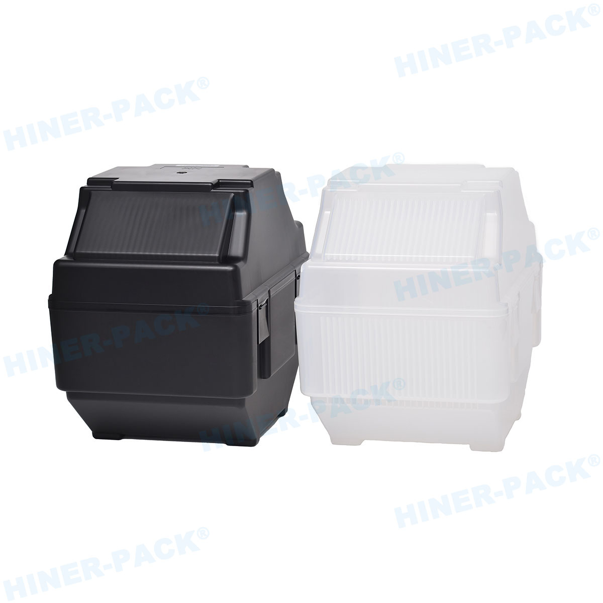
To maintain high wafer yields, every variable in the fabrication facility must be controlled. Selecting the correct carrier material and physical design is just as important as chemical purity in process baths or laser precision in lithography scanners. A carrier that deforms by even a fraction of a millimeter over its operating life can cause automated handling faults, leading to process tool shutdowns and expensive scrap events.
Protective solutions developed by Hiner-pack address the industry's most demanding physical and chemical protection needs, ensuring that wafers remain free of particulate and molecular contaminants throughout their processing lifecycle.
Securing your fab's productivity requires high-quality, reliable, and compliant carrier designs. Our engineering team is ready to evaluate your process parameters and provide customized carrier solutions that match your specific handling and thermal requirements. Reach out today to submit an inquiry, request technical datasheets, or coordinate sample testing with our application experts.
Choosing the right wafer carriers manufacturer ensures your advanced packaging operations run smoothly, protecting your high-value wafers at every step of the manufacturing journey.
Frequently Asked Questions (FAQ)
Q1: Why is selecting a specialized wafer carriers manufacturer vital for advanced nodes?
A1: Advanced process nodes are highly sensitive to microscopic contamination and minor mechanical shocks. A specialized manufacturer has the deep material science expertise and cleanroom production facilities required to produce carriers with tight dimensional tolerances, low outgassing properties, and reliable ESD protection, all of which directly prevent yield loss.
Q2: Which polymer is best suited for wafer carriers used in high-temperature processes?
A2: Polyetheretherketone (PEEK) is highly recommended for high-temperature applications. It exhibits excellent dimensional stability and maintains structural rigidity at temperatures exceeding 200°C, while producing minimal outgassing compared to other commodity polymers.
Q3: How do ESD-safe materials in wafer carriers protect semiconductor devices?
A3: ESD-safe carriers are made by compounding engineering polymers with carbon fibers or nanotubes, reducing surface resistivity. This allows static electricity to safely dissipate to ground, preventing electrostatic discharge events that can destroy delicate circuits and reducing electrostatic attraction that pulls airborne contaminants onto the wafers.
Q4: What SEMI standards are most applicable to wafer carriers?
A4: SEMI standards like SEMI E1.9 define the physical dimensions and interfaces for Front Opening Unified Pods (FOUPs), while SEMI M1 and related documents outline specifications for silicon wafers and the cassettes that hold them. Compliance with these standards ensures seamless integration with Automated Material Handling Systems (AMHS).
Q5: How can fabs prevent carrier-induced organic contamination on wafers?
A5: Fabs can prevent organic contamination by selecting carriers manufactured from virgin, high-purity polymers that have undergone post-mold vacuum baking. Additionally, using carriers with integrated nitrogen purging capabilities allows for a dry, inert micro-environment that prevents oxidation and airborne molecular contamination.














