
Advanced packaging architectures such as 2.5D/3D stacking, fan-out wafer-level packaging (FOWLP), and heterogeneous chiplet integration have pushed semiconductor manufacturing into a new phase. These structural breakthroughs bring severe operational difficulties to the cleanroom floor.
Thinned wafers under 50 micrometers suffer from extreme mechanical stress and thermal warpage. At the same time, high-density interconnections demand stricter particulate control and ESD safety. In this environment, your process carrier is no longer a simple plastic bin.
A wafer boat directly affects your line yield, wafer transfer stability, and production uptime. Choosing the right wafer boat supplier has become a critical strategic decision for process and procurement engineers. Established manufacturers like Hiner-pack are redefining performance benchmarks across the global supply chain.
Below are the six decisive qualities that separate top-tier wafer carrier manufacturers from standard container molders.
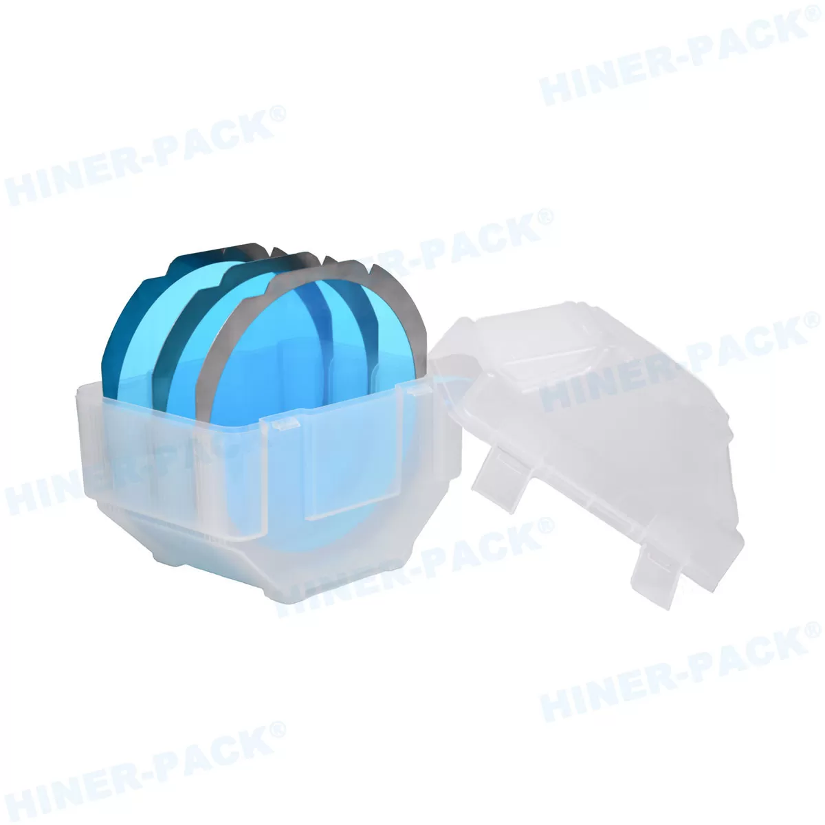
1. Proprietary Polymer R&D and Custom Material Compounding
Standard plastics cannot withstand modern backend assembly. Conventional catalog suppliers purchase commercial off-the-shelf resin pellets and mold generic carriers. In contrast, an elite wafer boat supplier operates an in-house polymer formulation facility.
High-performance wafer processing requires plastics engineered for specific chemical, mechanical, and thermal parameters. Advanced packaging steps involve repeated thermal cycles, aggressive solvent cleanings, and high-vacuum processing environments.
High-Temperature Resistance: Modern bake processes require carriers to endure continuous temperatures from 150°C up to 200°C without dimensional drift, slot sagging, or thermal deformation.
Ultra-Low Outgassing: Standard polymers release volatile organic compounds (VOCs) under heat. These chemicals condense on critical wafer patterns, ruining device performance. Custom-formulated polymers guarantee ultra-low outgassing under thermal vacuum tests.
Tailored Material Matrix: Leading manufacturers engineer compounds using Polyetheretherketone (PEEK), Polyethersulfone (PES), Perfluoroalkoxy (PFA), and specialized Polypropylene (PP) modified for thermal stiffness and chemical inertness.
Suppliers with dedicated polymer laboratories adjust reinforcement fibers, plasticizers, and stabilizers to meet the exact thermal and chemical profiles of your cleanroom line.
2. Precision and Non-Migratory ESD Protection
Electrostatic discharge (ESD) causes silent catastrophic failures in modern microelectronics. As transistor gate oxides become thinner and interconnect pitches shrink, even a tiny electrostatic pulse can destroy sub-micron circuits.
Budget carriers often rely on surface-coated antistatic agents. These surfactants attract ambient moisture to dissipate charges. Unfortunately, they rub off during mechanical handling, wash away in chemical baths, and migrate directly onto wafer active areas as ionic contamination.
A qualified wafer boat supplier implements volume-conductive and permanently dissipative compounds. They disperse carbon nanotubes, conductive carbon black, or inherently dissipative polymers (IDP) throughout the polymer matrix during raw material synthesis.
Stable Surface Resistivity: Maintaining a consistent resistance window across the entire carrier body (typically 104 to 109 Ω) eliminates both rapid spark discharge and slow charge accumulation.
Non-Sloughing Performance: Conductive additives remain locked inside the polymer chains, preventing carbon sloughing and particulate shedding during robot arm transfers.
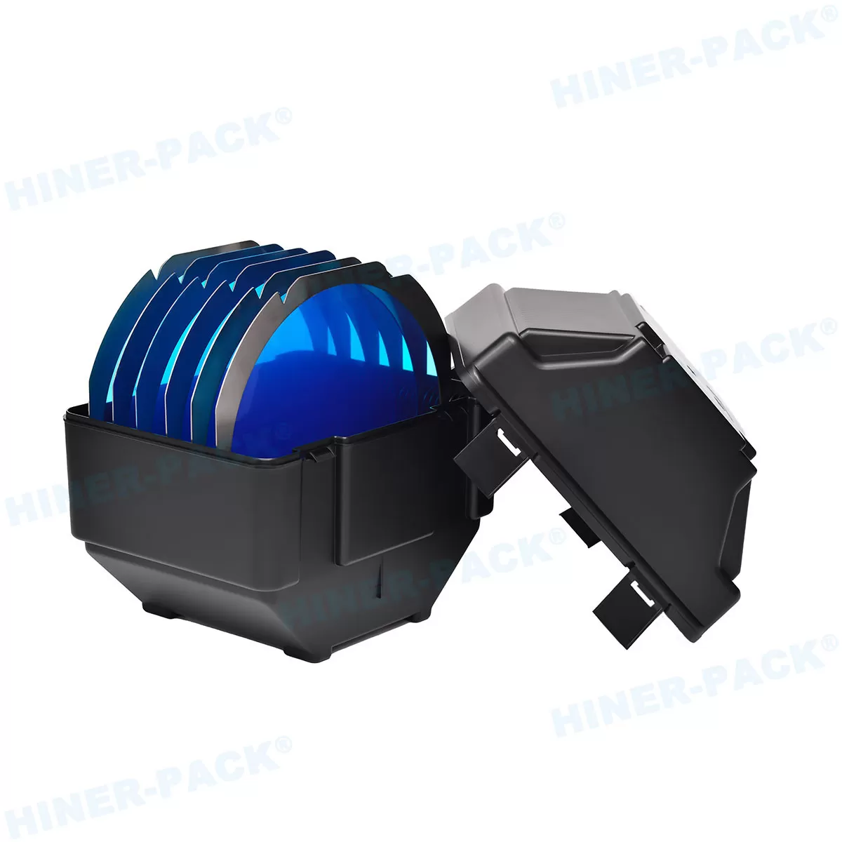
Visual Management Integration: Advanced compounding lets suppliers produce colored, ESD-safe carriers. This allows clear color coding for different process lines without sacrificing static safety.
Hiner-pack develops proprietary ESD-safe compounds that provide permanent electrostatic dissipation without introducing surface contamination or chemical migration risks.
3. Sub-Micron Tooling and Injection Molding Precision
A wafer carrier is a high-precision mechanical interface. When automated equipment handles hundreds of wafers per hour, tiny dimensional deviations cause catastrophic robotic transfer errors, edge chipping, or full wafer breakage.
High-level suppliers do not outsource mold manufacturing to third-party machine shops. Instead, they maintain dedicated mold-making facilities equipped with high-speed CNC machining centers, mirror electrical discharge machines (EDM), and optical coordinate measuring systems.
Tight Slot Pitch Tolerances: Every slot must maintain strict pitch spacing (often within ±0.05 mm) to align perfectly with automated wafer transfer systems.
Verticality and Flatness Control: Warped side rails cause uneven slot spacing. This imbalance exerts mechanical stress on thinned, warped silicon wafers during multi-wafer batch processing.
Advanced Shrinkage Compensation: High-performance engineering plastics exhibit complex volumetric shrinkage during cooling. True tooling experts compensate for polymer physics directly in the mold design.
Consistent tooling prevents batch-to-batch variation, ensuring that replacement carriers purchased years later match your original line qualifications down to the micron.
4. Seamless AMHS and Automation Compatibility
Modern semiconductor fabrication facilities and advanced OSAT lines rely heavily on Automated Material Handling Systems (AMHS), Automated Guided Vehicles (AGVs), and robotic end-effectors. Human operators rarely handle wafers manually.
An elite wafer boat supplier designs carriers strictly around international industry standards, such as SEMI specifications. Every external notch, robotic handling flange, and alignment track must interface cleanly with production automation.
Rigid Robotic Pick-Up Interfaces: The carrier must feature reinforced contact points that resist deflection when gripped by robotic end-effectors under maximum wafer payloads.
Consistent Kinematic Coupling: Bottom locator interfaces must drop accurately onto load ports, spin dryers, and transfer stations without mechanical binding or jitter.
Sensor-Friendly Geometries: Carrier walls and reference pockets must allow optical, capacitive, and photoelectric sensors to detect wafer presence and seating depth without false readings.
Suppliers that rigorously test physical automation interfaces prevent wafer drop accidents, pick-and-place alignment timeouts, and costly fab equipment stops.
5. Cleanroom Manufacturing and Stringent Particle Control
Sub-micron airborne particles can settle inside wafer active circuits, breaking metal lines or causing lithographic defocus. The packaging environment for high-end carriers must match the cleanliness of your own fabrication plant.
High-grade wafer boats are molded, inspected, and packed inside certified Class 100 (ISO Class 5) or Class 1000 (ISO Class 6) cleanrooms. Molding in uncontrolled warehouse spaces and rinsing products afterward is unacceptable for high-density IC manufacturing.
Automated Cleanroom Injection: Fully closed-loop electric injection machines minimize hydraulic oil mist and airborne dust in the production area.
Ultra-Pure Water (UPW) Ultrasonic Cleaning: Carriers undergo multi-stage ultrasonic baths using 18 MΩ·cm ultra-pure water to remove micro-particulates, ionic residues, and trace metals.
Vacuum Outgassing and Double-Bag Packaging: Cleaned carriers are vacuum-baked to eliminate residual volatile molecules, then vacuum-sealed in cleanroom-grade, anti-static double bags.
This strict level of hygiene ensures that carriers arrive on your line ready for immediate wet processing, baking, or vacuum handling without extra pre-wash cycles.
6. Turnkey Customization (OEM/ODM) and Full Product Ecosystem
Standard off-the-shelf catalog products rarely fit emerging advanced packaging lines. Compound semiconductors (such as SiC and GaN), ultra-thin wafers with thick polyimide layers, and unusual substrate thicknesses require customized carrier profiles.
An exceptional wafer boat supplier acts as an extension of your research and development team. They provide full OEM and ODM support, turning specialized engineering drawings into functional prototypes within days.
Rapid Prototyping: Rapid mold sampling and 3D precision verification let engineers validate custom slot depths and structural pockets before volume tooling.
Custom Dimensions: Full engineering capability to build 4-inch, 6-inch, 8-inch, and 12-inch carriers, alongside customized carriers for irregular panels and diced substrate frames.
Complete Handling Ecosystem: Beyond wafer boats, a comprehensive supplier manufactures matching horizontal shipping boxes, wafer jars, process cassettes, JEDEC matrix trays, IC chip trays, and vacuum release gel boxes.
Sourcing your process carriers and backend shipping supplies from a single qualified manufacturer simplifies qualification audits, unifies quality standards, and cuts logistics costs.
Why Partner with Hiner-pack?
Founded in 2013, Hiner-pack has grown into a leading technology-driven manufacturer dedicated to semiconductor packaging, wafer handling, and electronic protection solutions.
Hiner-pack operates an integrated material modification center alongside precision mold manufacturing and cleanroom injection lines. With dozens of technical patents and specialized polymer formulations, the company delivers dependable ESD-safe carriers to top-tier semiconductor fabs and OSATs across the globe.
The company maintains a broad product catalog, covering high-temperature wafer boats, front-opening shipping boxes, process cassettes, precision JEDEC matrix trays, and vacuum-release gel boxes. Hiner-pack gives cleanroom operations the material stability and dimensional accuracy required for next-generation packaging lines.
Frequently Asked Questions (FAQ)
Q1: What is the main difference between a wafer boat and a wafer cassette?
A1: While both hold wafers in parallel slots, wafer boats (or process boats) are typically designed for high-temperature furnace steps, chemical wet benches, and harsh internal cleanroom processing. Wafer cassettes generally refer to carriers optimized for storage, automated machine loading, and transport between different production bays.
Q2: Why are standard antistatic sprays unsuitable for wafer carriers in advanced packaging?
A2: Topical antistatic coatings easily rub off, degrade over time, and wash away in chemical baths. Even worse, the chemical surfactants in sprays release free ions and volatile contaminants directly onto wafer surfaces. Advanced packaging lines require permanently dissipative polymers compounded throughout the material matrix.
Q3: How does polymer outgassing damage semiconductor wafers during baking?
A3: When a plastic carrier is exposed to temperatures between 100°C and 200°C, low-molecular-weight additives can vaporize. In vacuum ovens or closed chambers, these volatile molecules redeposit onto the bare silicon or metal pads. This creates thin chemical films that cause wire-bonding peeling, poor metal adhesion, and optical defects.
Q4: Can a wafer boat supplier produce carriers for non-standard wafer thicknesses?
A4: Yes. An elite wafer carrier manufacturer with in-house tooling can modify slot pitch, slot width, and pocket profiles. This accommodates ultra-thinned bonded wafers, warped substrates, or extra-thick multi-layer composite structures without mechanical binding.
Q5: What cleaning and packaging protocols should I demand before purchasing wafer boats?
A5: You should verify that the supplier uses multi-stage ultrasonic cleaning with 18 MΩ·cm ultra-pure water (UPW), cleanroom-grade drying, and particle inspection inside an ISO Class 5 or Class 6 environment. Finished carriers must be double-bagged in static-shielding, non-outgassing cleanroom bags.
Upgrade Your Wafer Handling Reliability Today
Your microelectronic components deserve carrier protection that prevents yield loss, static damage, and mechanical failure. Relying on generic plastic containers puts your cleanroom throughput and device performance at serious risk.
Partner with an experienced wafer boat supplier that understands precision tooling, high-purity polymer chemistry, and automated fab requirements. Contact the engineering team at Hiner-pack today to discuss your project requirements, request a custom design review, or order qualification samples.














