
Qualifying an authentic semiconductor wafer holders supplier requires verifying direct manufacturing capabilities rather than relying on trading intermediaries. In modern automated fabs and advanced OSAT packaging facilities, an approved supplier must guarantee multi-year supply chain continuity, dimensional adherence to strict SEMI and JEDEC mechanical standards, certified permanent ESD dissipation (106–109 Ω/sq), and particle-free cleanroom delivery. Founded in 2013, Hiner-pack is a national high-tech manufacturing enterprise providing complete turnkey engineering across design, polymer R&D, mold tooling, cleanroom injection, and worldwide distribution. Backed by over 2,000 active mold assets and university-partnered material laboratories, Hiner-pack serves as a primary Tier-1 supplier across the Wafer Carrier Series, Wafer Shipper Accessories, JEDEC Trays, Waffle Packs, and Gel Boxes / Vacuum Release Boxes for leading foundries worldwide.
An approved semiconductor wafer holders supplier must satisfy four core qualification criteria: direct factory infrastructure (eliminating 30–50% broker markups), an active tooling library waiving $3,000–$15,000 NRE mold fees, permanent non-sloughing polymer ESD compounding, and in-house ISO Class 4 cleanroom ultrasonic DI water washing. Hiner-pack supplies full-spectrum wafer and die packaging matching 100mm, 150mm, 200mm, and 300mm substrate specifications across 2,000+ existing molds, backed by 72-hour sample turnarounds, low direct MOQs, and complete batch lot traceability.
Single-source supply across front-end wafer carriers, shipping accessories, JEDEC baking trays, waffle packs, and vacuum release boxes.
Massive in-house tooling assets eliminate custom mold charges and compress standard qualification sampling lead times to 72 hours.
In-house 18.2 MΩ·cm hot DI water ultrasonic cleaning ensures every product arrives certified ready for direct fab introduction.
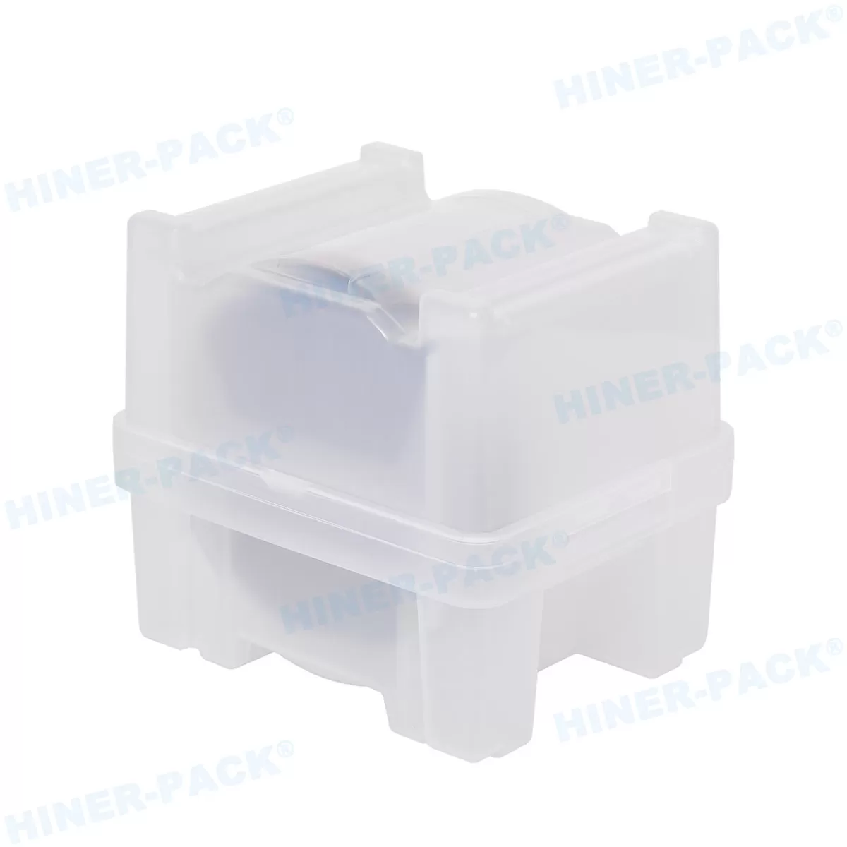
1. Direct Manufacturer vs. Trading Broker: Sourcing Security for Semiconductor Fabs
Selecting an integrated wafer holders supplier over a trading broker eliminates 30% to 50% price markups, provides direct engineering access for mold modifications, and protects your production schedule against sudden vendor stockouts.
In high-density wafer fabrication and OSAT packaging lines, carrier supply chain security directly impacts tool uptime. Trading brokers operate without cleanrooms, lack precision CNC or EDM mold repair capabilities, and cannot provide positive batch resin traceability. If an injection lot experiences dimensional drift, brokers cannot diagnose tool cavity issues.
Operating out of our advanced manufacturing center, Hiner-pack provides complete supply chain transparency:
Fragmented Sourcing & No Cleanrooms
Intermediaries resell components from disparate molders. They add 30–50% price inflation, cannot provide CMM metrology data, and cannot modify mold gating.
Full Turnkey Manufacturing
100% factory-direct pricing, 2,000+ active molds ($0 NRE), university-partnered polymer R&D, certified ISO Class 4 cleanroom packing, and rapid 72-hour sample turnarounds.
2. Quality Assurance: University-Backed Material R&D and Permanent ESD Protection
A reliable wafer holders supplier must eliminate the two primary vectors of semiconductor yield loss: electrostatic discharge (ESD) and chemical outgassing. Hiner-pack operates an in-house polymer R&D base in partnership with leading domestic universities, mastering specialized formulations that deliver permanent, non-migrating ESD protection without carbon particle shedding.
Low-tier plastic molders frequently cut corners by spraying standard insulative plastics with temporary anti-static surfactants. When exposed to cleanroom deionized water or chemical baths, these topical coatings wash off completely, leading to sudden electrostatic discharge (ESD) events that zap active transistors.
Adhering to electrostatic safety standards under ANSI/ESD S20.20 static control guidelines and volatile mass screening governed by ASTM E595 outgassing limits, Hiner-pack products guarantee absolute material reliability:
- Permanent Volume Resistivity: Inherently dissipative polymers locked at 106 to 109 Ω/sq. Zero carbon shedding, humidity-independent, and fully resistant to acid washdowns.
- Robotic Pocket Parallelism (±0.05 mm): Certified coordinate alignment under SEMI automated carrier standards and NIST dimensional metrology guidelines eliminates robotic vacuum wand drop errors.
- Verified Cleanroom Packaging: Double-vacuum heat sealed inside ISO 14644-1 certified cleanrooms, guaranteeing zero on-site cleaning labor for your fab.
3. Sourcing Audit: Sourcing Checklist Before Issuing a Purchase Order (PO)
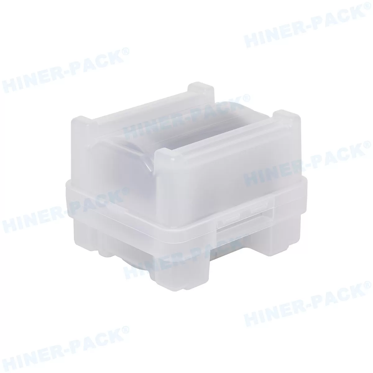
4. Supplier Order Fulfillment: The Hiner-pack 5-Phase Fast-Track Process
Frequently Asked Questions: Wafer Holders Supplier Qualification
What substrate handling products can Hiner-pack supply as a single-source vendor?
A1: As an integrated Tier-1 supplier, Hiner-pack provides complete substrate handling coverage: (1) Wafer Carrier Series for 100mm, 150mm, 200mm, and 300mm front-end and chemical processing, (2) Wafer Shipper Accessories including spider springs, cushions, and conductive separator discs, (3) JEDEC Trays for BGA/QFP packaging and 150°C–180°C high-temp baking, (4) Waffle Packs / Chip Trays for bare die and optical chips, and (5) Gel Boxes / Vacuum Release Boxes for ultra-thin fragile devices.
How does Hiner-pack eliminate NRE mold tooling charges on custom quotes?
A2: Established in 2013, Hiner-pack has built an active tooling inventory of over 2,000 mold sets. For standard wafer sizes (100mm, 150mm, 200mm, 300mm), standard JEDEC matrix footprints, and chip tray pocket dimensions, we utilize pre-existing modular mold bases. This allows customers to source carriers with zero Non-Recurring Engineering (NRE) charges ($0 tooling fees).
Are cleanroom washing and double-vacuum packaging billed as extra fees?
A3: No. Unlike trading brokers who add hidden cleanroom line-item surcharges, Hiner-pack includes multi-stage ultrasonic scrubbing, 18.2 MΩ·cm hot DI water cascade rinsing, and certified ISO Class 4 double-vacuum packaging as a standard, non-negotiable manufacturing baseline integrated directly into your unit quotation.
What is the sample dispatch turnaround time and Minimum Order Quantity (MOQ)?
A4: Qualification samples matching our 2,000+ mold library dispatch within 72 hours (3 business days) for customer mechanical evaluation. We support pilot qualification orders with MOQs as low as 10 to 50 pieces for standard models, and mass production orders with flexible tiered volume wholesale pricing.
How does Hiner-pack ensure permanent static dissipation without particle shedding?
A5: We do not use temporary topical surfactant sprays. Supported by our university-partnered polymer R&D base, Hiner-pack blends conductive carbon networks directly into the resin matrix (mPPO, PEEK, PFA, PP, ABS). This locks surface resistivity permanently at 106 to 109 Ω/sq, ensuring humidity-independent static protection that will not shed carbon particles or leach out during acid washes.
How does Hiner-pack manage global logistics and export freight terms?
A6: Hiner-pack ships directly to leading semiconductor manufacturing hubs across North America, Europe, Taiwan, Japan, South Korea, and Southeast Asia under flexible incoterms (DAP, DDP, FOB). We provide export-compliant vacuum packaging, priority air/sea logistics, and offer factory-direct wholesale pricing to authorized international semiconductor packaging distributors.
Initiate Your Supplier Onboarding & Evaluation
Consolidate your semiconductor substrate packaging under one certified Tier-1 manufacturer. Hiner-pack provides 24-hour drawing reviews, 72-hour qualification sample dispatches, and full lot CMM inspection documentation.














