
In semiconductor wafer fabrication and assembly processes, wafer trays are not the most expensive equipment. Yet they directly affect product yield and operational efficiency. A single wafer moves through dicing, grinding, testing, and final packaging. Each transfer, temporary storage, and transport step carries risks: particle contamination, mechanical scratches, or electrostatic discharge (ESD) damage.
A quality wafer tray must provide safe, stable physical support. It also needs to meet multiple engineering requirements: cleanroom compatibility, ESD protection, temperature resistance, and reusability. When production expands or equipment upgrades occur, the ability to obtain sufficient trays with correct specifications quickly determines whether your line faces idle downtime.
This is where Hiner-pack delivers real value. As a high-tech enterprise focused on automated wafer handling, carrying, and transport solutions, Hiner-pack combines deep polymer material R&D with strong mold processing capabilities. Through large-scale finished goods inventory and a global logistics network, we offer a "order now, ship now" experience. Our wafer trays factory operates with one clear goal: keep your production moving without interruption.
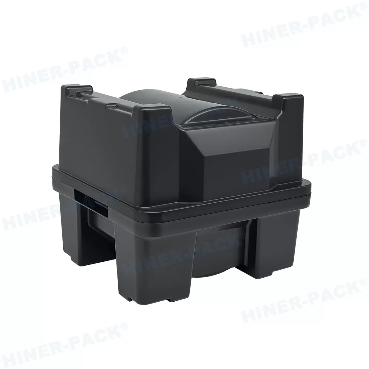
Why Material and Process Directly Impact Wafer Yield
Lower-tier trays use standard plastics with simple injection molding. They carry hidden risks that cost you yield.
Contamination from outgassing: Inferior materials release volatile organic compounds (VOCs) or microscopic particles under heat or over time. These contaminants settle on wafer surfaces and ruin devices.
Poor ESD control: Unstable surface resistivity fails to dissipate static charge. A single discharge can zap sensitive circuits, causing latent failures or immediate rejects.
Dimensional instability: Uncontrolled shrinkage leads to warped trays or misaligned slots. Wafers shift, edges collide with pocket walls, and micro-cracks form.
Low durability: After repeated cleaning and use, cheap trays develop cracks, burrs, or surface roughness. Replacement frequency rises, and so does your hidden cost per wafer.
Hiner-pack started its journey in 2013. We have stayed focused on semiconductor packaging materials ever since. Our team mastered specialized processing and manufacturing technologies. We co-established a polymer material R&D base with well-known domestic universities and research institutes. At the molecular level, we optimize heat resistance, anti-static performance, and low-extraction characteristics. Every tray that leaves our wafer trays factory meets the strict standards of the semiconductor industry.
Material Selection: PP, PEEK, PC, and More
Different applications call for different base resins. Polypropylene (PP) offers cost-effectiveness and good chemical resistance for general use. Polyether ether ketone (PEEK) withstands higher temperatures and aggressive solvents, suitable for advanced packaging. Polycarbonate (PC) provides optical clarity and impact strength.
Hiner-pack's material science team evaluates each resin's properties against your specific process conditions. We adjust additives for ESD control without compromising cleanliness or mechanical strength. The result: a tray that performs consistently across thousands of cycles.
Ready Stock + Global Fast Shipping – Solving the Delivery Dilemma
In semiconductors, lead time is a competitive weapon. Equipment arrives on-site, but trays are missing. Or urgent capacity expansion kicks off, and your supplier quotes a four-week delivery window. These scenarios happen more often than they should.
Hiner-pack understands this pain point firsthand. We built a large-scale finished goods inventory covering the most popular wafer tray sizes. Our stock includes 2-inch, 4-inch, 6-inch, 8-inch, and 12-inch standard formats, along with many non-standard custom models. This wafer trays factory maintains real-time inventory data through our smart warehousing system.
Once you confirm your order, our team moves into packing and shipping immediately. Our global fast shipping capability rests on three pillars:
Smart warehouse operations: Real-time stock updates eliminate manual verification delays.
Multi-modal logistics network: Long-term partnerships with international carriers give you options – air, sea, or express courier.
Customs clearance expertise: We handle semiconductor consumables export/import paperwork daily. Standardized documentation reduces port-of-entry holdups.
Whether your facility sits in Southeast Asia, Europe, North America, or elsewhere, Hiner-pack delivers quality trays in the shortest possible time. Our wafer trays factory turns inventory into motion – fast.
Emergency Production Support
What happens when your line faces a sudden tray shortage? We set aside a portion of our stock specifically for emergency orders. Our team prioritizes these requests and coordinates with logistics partners to expedite shipment. This proactive approach has earned us trust from fabs and OSATs that cannot afford a single hour of idle time.
2000+ Existing Mold Library – OEM/ODM Without Waiting for New Tooling
Wafer trays are not one-size-fits-all. Your wafers differ in diameter, thickness, slot count, material preference (PP, PEEK, PC, etc.), and cleanliness grade. If every custom order required fresh mold development, lead times and costs would spiral.
Hiner-pack maintains a mold library with over 2,000 existing tooling sets. This collection covers the majority of standard and derivative configurations used in the industry.
For standard requirements, we ship directly from stock. For non-standard sizes or unique structures, our mold library offers a solid starting point. We adapt existing designs rather than starting from scratch. This approach slashes new mold development time significantly.
Our OEM/ODM service covers the entire journey: material selection, structural design, prototyping, and volume production. We support custom drawings, co-development projects, and private label branding. A dedicated engineering team manages each project from concept to delivery.
This "mold-base as foundation, rapid response as engine" model has made Hiner-pack a preferred partner for many well-known semiconductor companies worldwide. Our wafer trays factory operates with flexibility that few competitors can match.
Case Example: Quick Turnaround for Non-Standard Tray
A customer needed a 300mm tray with a specialized pocket geometry for thin wafers. Our engineering team reviewed the mold library, identified a close match, and modified the cavity design. Within 10 days, we shipped functional samples. The customer approved them after a single iteration. Full production followed two weeks later. This speed would have been impossible without our extensive mold inventory.
Cleanroom Compatibility and Reusability – Lowering Cost Per Use
Semiconductor manufacturing demands ultra-clean environments, typically ISO Class 5 (Class 100) or higher. Hiner-pack designed its wafer trays with cleanroom compatibility at the core.
Our materials show low particle generation and low outgassing. We validate cleanliness through actual testing in controlled environments. Surface finishes are smooth, with no sharp edges that could trap particles or damage wafers. The structural design avoids dead corners where contaminants accumulate. Cleaning is straightforward – our trays withstand ultrasonic cleaning, IPA wiping, and standard semiconductor-grade detergents.
Reusability matters equally. Hiner-pack trays offer excellent mechanical strength and chemical resistance. They maintain dimensional stability and surface integrity after multiple wash cycles. This durability translates directly to a lower cost per use (CPU). Instead of treating trays as consumables, you treat them as long-life assets.
Our wafer trays factory builds this reusability into every product. We know that your operational economics depend not just on the purchase price, but on the total cost over the tray's service life.
Environmental and Operational Benefits
Longer tray life reduces waste generation and procurement frequency. Fewer shipments mean lower carbon footprint. Less frequent ordering also reduces your administrative overhead. These advantages align with the industry's growing focus on sustainability without compromising performance.
R&D Strength and University Partnerships – Innovation Backed by Patents
Hiner-pack's R&D capability did not appear overnight. We have invested continuously in polymer material science and precision injection molding over the past decade. Our joint laboratories with domestic universities and research institutes serve as innovation hubs.
We hold multiple invention and utility model patents covering material formulations, structural designs, and manufacturing processes. These patents protect our technology and provide you with compliance assurance. When you source from our wafer trays factory, you benefit from proven, legally protected solutions.
Our R&D team stays ahead of industry trends. Wafer thinning, large-diameter wafers (12 inches and above), and advanced packaging methods like Fan-Out and 3D stacking require new tray designs. We develop products that match these emerging process requirements. We do not wait for market demand to mature – we anticipate it.
Material Science Innovations
One recent development involves a modified PEEK compound that reduces ionic contamination by 40% compared to standard grades. Another project produced a PP-based material with improved ESD stability across varying humidity levels. These innovations come directly from our university collaboration programs. They translate into measurable yield improvements for our customers.
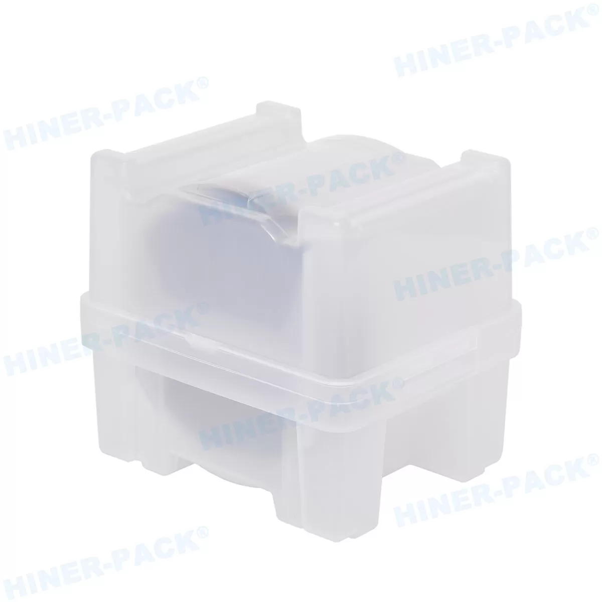
Clean Manufacturing Environment and Rigorous Quality Control
Our wafer trays factory features advanced mold processing and injection molding equipment. We operate high-standard cleanroom washing lines and maintain a full suite of inspection instruments. From raw material receiving, through injection molding, cleaning, packaging, and final shipping – every step follows strict quality control protocols.
Our production environment ensures that trays leave the factory at the cleanliness level required for semiconductor manufacturing. This approach reduces the burden of secondary cleaning at your facility. Our inspection equipment includes dimensional measurement tools, surface resistivity testers, and particle counters. We verify batch consistency and maintain full traceability.
Quality is not a department at Hiner-pack – it is a discipline. Every operator, every technician, and every engineer understands that our trays carry wafers worth thousands of dollars each. A single defect is unacceptable.
Traceability and Documentation
Each batch of trays receives a unique lot number. We retain production records, material certificates, and test reports for every lot. If you ever need to trace a performance issue back to a specific production run, we can do it. This traceability supports your own quality management systems and regulatory compliance.
Global Distributors Wanted – Partner with Hiner-pack
Hiner-pack is expanding its global distribution network. We invite partners who serve the semiconductor industry to join us. Our distributor program offers:
Competitive pricing structures with attractive margin potential
Stable stock availability and flexible delivery schedules
Technical support and marketing collateral for your sales team
OEM/ODM collaboration to help you build your own private label brand
If you have customer relationships in the semiconductor supply chain and the ability to provide local service, we want to talk. Our wafer trays factory provides the product foundation. You provide the local market expertise. Together, we build a winning partnership.
Ideal Distributor Profile
We look for distributors with experience in semiconductor consumables, cleanroom supplies, or automation components. Technical knowledge of wafer handling is a plus. We also value partners who can offer value-added services like local warehousing, kitting, or just-in-time delivery. If this sounds like you, reach out.
Conclusion – Choose Hiner-pack for Stock, Speed, and Quality
In the specialized field of wafer trays, Hiner-pack has spent over a decade refining its expertise. We combine material R&D, mold engineering, inventory management, and global logistics into a single cohesive supply system. Our wafer trays factory delivers rapid response, worldwide shipping, and uncompromising quality.
Whether you operate a wafer foundry, an assembly and test facility, or an equipment integration business, Hiner-pack deserves a place on your preferred supplier list. We do not just sell trays – we protect your wafers and your production schedule.
When you search for a wafer trays factory that understands the full context of semiconductor manufacturing, look no further. Hiner-pack is ready to serve.
Frequently Asked Questions (FAQ)
Q1: What standard wafer sizes does Hiner-pack support, and do you offer custom sizes?
A1: We stock trays for 2-inch, 4-inch, 6-inch, 8-inch, and 12-inch wafers as standard. For custom sizes, our 2,000+ mold library allows rapid adaptation. We also support full OEM/ODM development for unique dimensions, pocket geometries, and material specifications.
Q2: How does Hiner-pack ensure ESD protection in its wafer trays?
A2: We incorporate static-dissipative additives into our base resins during compounding. Our finished trays meet surface resistivity requirements typically between 10⁶ and 10¹¹ ohms per square. We test each batch using calibrated instruments and provide ESD performance documentation with every shipment.
Q3: What is your typical lead time for stock items versus custom orders?
A3: Stock items ship within 24 to 48 hours after order confirmation. Custom orders using existing mold modifications typically require 10 to 15 days for samples and 3 to 4 weeks for full production. New mold development takes longer, but our extensive library minimizes this scenario.
Q4: Are your wafer trays compatible with automated wafer handling systems?
A4: Yes. We design our trays with standard industry dimensions and tolerances that work with most automated transfer and storage equipment. For specific automation interfaces, we can adjust pocket pitch, stacking features, and alignment keys to match your system requirements.
Q5: How can I become a distributor for Hiner-pack?
A5: Reach out to our sales team through the contact form on our website. We will schedule a discovery call to understand your market coverage, customer base, and service capabilities. From there, we propose a distribution agreement tailored to your region and business model.
Ready to secure your wafer tray supply chain? Contact Hiner-pack today to request samples, discuss your specific requirements, or explore distributor opportunities. Our team responds within 24 hours with a tailored solution. Inquire now and keep your production running without interruption.














