
In semiconductor fabrication and advanced packaging, the margin for error is zero. A single microscopic electrostatic discharge (ESD) event, outgassing contamination, or vibration-induced edge chipping can destroy thousands of dollars worth of processed silicon wafers. Whether you are handling 2-inch compound semiconductor substrates (SiC/GaN) or high-density 12-inch wafers, choosing the right wafer tray is a critical yield-protection strategy.
If you are currently evaluating wafer trays for sale, this technical guide covers the essential engineering parameters—including polymer selection, ESD protection levels, cleanroom standards, and automation compatibility—to ensure your substrates remain intact from fab to final packaging.
Need to test mechanical fit and ESD resistance? Request Free Wafer Tray Samples from Hiner-pack (Dispatches in 48 Hours).
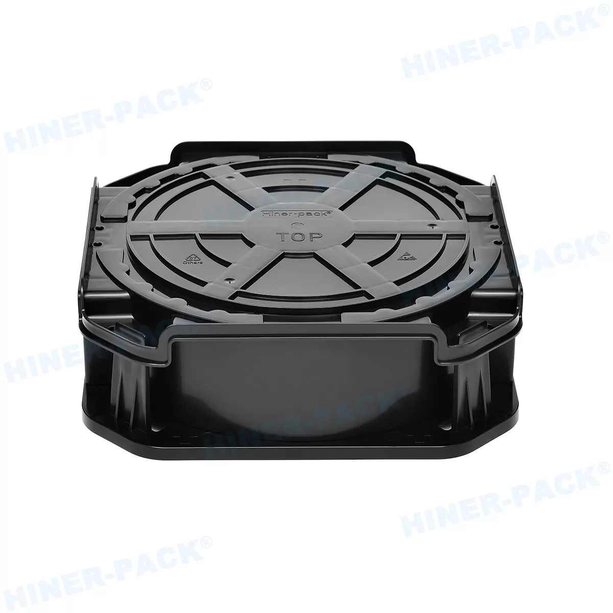
1. Key Material Selection Criteria: Matching Tray Polymers to Process Demands
The performance of a wafer carrier depends heavily on its polymer formulation. When selecting wafer packaging, engineers must balance thermal stability, mechanical stiffness, and electrostatic control.
At Hiner-pack, our dedicated Polymer Material R&D Center (developed in partnership with research institutions) manufactures specialized formulations tailored to specific fab environments:
| Material Type | Surface Resistivity (Ω/sq) | Max Temp Rating | Primary Use Case | Key Features |
|---|---|---|---|---|
| Conductive PP (Polypropylene) | 10^4 - 10^6 | ~80°C | Shipping & In-Plant Transport | High impact resistance, cost-effective, continuous static dissipation |
| High-Temp Engineered Plastics (PEEK/PES) | 10^6 - 10^9 | 150°C - 200°C+ | In-Process Baking / Vacuum Cure | Ultra-low outgassing, high dimensional stability under heat |
| Transparent Antistatic PS/PET | 10^9 - 10^11 | ~60°C | Inspection & Die Storage | Optical clarity for visual inspection without opening the tray |
| Custom Modified Polymers | Tailored to Spec | Up to 180°C | Automated Handlers / OEM | Patented composite formulations with custom coloration for lot tracing |
2. Static Control: Permanent ESD vs. Temporary Surface Coatings
For semiconductor manufacturing, temporary antistatic coatings pose a severe contamination risk. Surfactant-coated plastics rely on ambient humidity to dissipate charges and can degrade over time, leading to unexpected electrostatic discharge or chemical residue transfer onto the wafer surface.
When searching for wafer trays for sale, verify that your supplier uses inherently dissipative or conductive polymers:
ANSI/ESD S20.20 Compliance: Hiner-pack's raw materials feature permanently blended conductive matrix networks, ensuring that surface resistivity (10^4 - 10^9 Ω/sq) remains constant regardless of humidity, wash cycles, or storage duration.
Low Outgassing: High-grade polymers prevent volatile organic compounds (VOCs) from depositing onto sensitive wafer surfaces during storage.
3. Automated Handling and Precision Mold Tooling
Modern automated test and assembly equipment requires strict dimensional tolerances. Warped or out-of-spec trays lead to vacuum pickup errors, machine jams, and edge chipping.
Precision CNC & EDM Tooling: Ensures slot pitch, pocket depth, and robotic alignment notches strictly follow standard industry profiles.
Minimal Warpage: Optimized injection parameters ensure dimensional stability across temperature variations.
Low-Particle Retention: Specially finished cavity surfaces minimize friction and prevent particle generation during loading and transit.
4. Comprehensive Carrier Portfolio by Hiner-pack
Founded in 2013 in Shenzhen, China, Hiner-pack provides integrated turnkey design, mold tooling, and injection manufacturing for semiconductor carriers across multiple formats:
Wafer Carrier Series: Single Wafer Shippers (2", 3", 4", 6", 8", 12"), Multi-wafer Cassettes, and Coin-Style Boxes.
Wafer Shipper Accessories: Cleanroom-grade cushioning sponges, conductive separator sheets, gaskets, and retention springs.
JEDEC Trays & IC Trays: High-temperature bakeable matrix trays for QFN, BGA, CSP, and packaged modules.
Waffle Packs & Chip Trays: High-precision pocket trays designed for bare die, optical chips, and sensors.
Gel Boxes & Vacuum Release Boxes: Non-contact surface retention packaging for fragile, thinned dies.
5. Direct Manufacturer Advantages: Why Source from Hiner-pack
Sourcing directly from an established manufacturer eliminates distributor markups, reduces lead times, and allows for technical customization:
One-Stop Turnkey Production: From custom raw material compounding to mold manufacturing and cleanroom injection, all processes are managed in-house.
Proprietary Material Patents: Multiple invention and utility patents covering static control and high-temperature polymer modifications.
Custom OEM/ODM Services: Tailored cavity dimensions, custom pocket matrices, and colored anti-static formulations for visual lot management.
Quality Control Equipment: In-house optical coordinate measuring machines (CMM), ESD resistance meters, and cleanroom particulate monitoring.
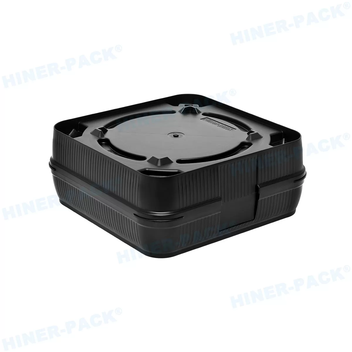
3-Step Engineering Verification: Free Samples & CAD Package
We understand that semiconductor handling requires rigorous qualification before volume procurement. Hiner-pack provides engineers and procurement managers with a complete verification kit to evaluate material compatibility, automated handling fit, and ESD integrity.
What Your Evaluation Package Includes:
Functional Test Samples: 2 to 5 free sample trays/carriers configured to your wafer or chip dimensions.
CAD & 3D Models: Instant access to .STEP / .IGS / .DXF drawing files for your mechanical simulation.
Full Compliance Dossier: Official test reports for ESD surface resistivity, RoHS, REACH, and outgassing data.
Direct Engineering Feedback: 1-on-1 consultation with our mold and polymer R&D team for custom tooling needs.
How to Request Your Kit:
Specify Your Parameters: Email your target wafer diameter (e.g., 4", 8", 12"), substrate thickness (μm), and process temperature to our engineering team.
Sample Dispatch: Standard stock samples are prepared in our cleanroom and shipped via DHL/FedEx within 48 hours.
Receive Factory-Direct Pricing: Along with your samples, receive a tiered volume quotation with transparent lead times.
Fast-Track Contact Channels:
Engineering Email: rainbowzhu@hiner-pack.com / cathyxing@hiner-pack.com (Typical reply time: Under 2 hours)
Instant Technical Chat: Message our technical team directly via WhatsApp for urgent project inquiries.
Custom OEM / Tooling Inquiries: Provide your proprietary die/wafer drawings for a formal DFM (Design for Manufacturability) analysis within 1 business day.
Frequently Asked Questions About Wafer Trays for Sale
Q1: What types of wafer trays for sale does Hiner-pack offer, and what is the minimum order quantity (MOQ)?
A1: Hiner-pack manufactures a complete portfolio of semiconductor handling products, including single wafer shippers (2", 3", 4", 6", 8", 12"), multi-wafer storage cassettes, coin-style boxes, high-temperature JEDEC matrix trays, and precision waffle packs for singulated bare dies. For standard catalog wafer trays for sale, we support low-volume evaluation orders starting from 10 to 50 units. For fully customized OEM pocket molds, volume pricing and batch MOQs are calculated based on mold cavity design and polymer specifications.
Q2: How do I ensure the wafer trays for sale meet my facility's ESD and thermal baking requirements?
A2: All Hiner-pack wafer carriers utilize inherently conductive or static-dissipative polymers with permanent surface resistivity ranging from 10^4 to 10^9 Ω/sq, fully compliant with ANSI/ESD S20.20 standards. If your process requires high-temperature baking or vacuum degassing, we offer specialized engineered resins (such as modified PES or PEEK blends) capable of continuous thermal resistance up to 150°C - 200°C+. Every shipment includes a certified certificate of analysis (COA) detailing ESD resistance and thermal tolerances.
Q3: Can Hiner-pack customize wafer trays for fragile, non-standard, or compound semiconductor substrates?
A3: Yes. Beyond standard silicon wafers, our in-house mold R&D team engineers custom carriers specifically optimized for Silicon Carbide (SiC), Gallium Nitride (GaN), glass substrates, lithium tantalate, and ultra-thin wafers (<100 μm). Custom pocket profiles, edge-retention features, and non-contact surface designs prevent crystal micro-cracking and edge chipping during high-speed transit.
Q4: How does Hiner-pack ensure cleanroom compliance and contamination control for purchased wafer carriers?
A4: Particle contamination and volatile outgassing are strictly controlled throughout our manufacturing process. Trays are molded using high-purity virgin resins on dedicated injection lines, processed through multi-stage ultrasonic cleaning systems, and double-vacuum bagged within an ISO-certified cleanroom environment. This guarantees our wafer trays for sale arrive ready for immediate cleanroom introduction without risk of cross-contamination.
Have additional technical requirements or need custom tooling? Contact our engineering team directly at rainbowzhu@hiner-pack.com / cathyxing@hiner-pack.com for fast technical support and direct factory quotations.














