
As the global semiconductor industry continues its robust expansion through 2026, wafer trays and related carriers have become indispensable consumables in chip manufacturing. The worldwide semiconductor carrier market is projected to surpass $5 billion in 2026, with FOUP (Front Opening Unified Pod) and FOSB (Front Opening Shipping Box) capturing the largest share for 300mm wafer processing and transportation. From wafer dicing, grinding, and polishing to photolithography, etching, deposition, testing, and final packaging, wafer trays play a dual role as both protector and transporter. A single wafer can be worth hundreds or even thousands of dollars, and its yield and safety depend heavily on the cleanliness, precision, and reliability of the carrier.
For procurement teams and process engineers, however, the real challenge lies in distinguishing truly capable wafer trays manufacturer from the many suppliers flooding the market. Which brands genuinely deliver on material science, precision molding, and cleanroom compatibility? Who offers the most comprehensive product portfolios and responsive technical support? This article draws on the latest 2026 industry data, combining technical capabilities, product performance, customer feedback, and market share to rank the top ten FOUP and FOSB manufacturers. We will also examine why one-stop solution providers like Hiner-pack are gaining traction among leading semiconductor fabs and OSATs.
Selection Criteria: How We Define a Leading Wafer Trays Manufacturer
Before presenting our ranking, we clarify the six core dimensions that guided our evaluation. These criteria ensure that we recognize manufacturers who truly excel in both technical depth and practical service.
R&D Capability: Mastery of polymer modification, precision injection molding, and cleanroom processing; number of patents and R&D investment ratio.
Product Performance Metrics: Cleanliness class (ISO Class), particle generation, outgassing control, ESD protection, dimensional accuracy, and seal integrity.
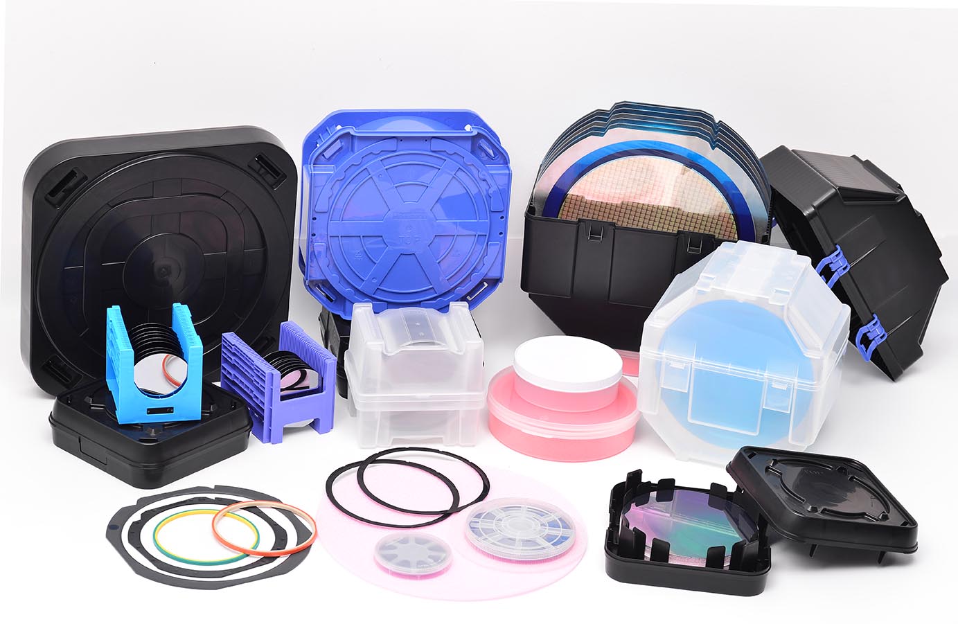
Product Line Completeness: Coverage of FOUP, FOSB, wafer cassettes, wafer trays, reticle pods, wafer rings, and other carrier types.
Quality Management System: ISO 9001, ISO 14001, IATF 16949 certifications; robust incoming inspection, in-process control, and outgoing testing procedures.
Customer Service & Technical Support: Custom design capabilities, rapid after-sales response, and professional technical consultation and training.
Sustainability & Cost-Effectiveness: Reusable design approaches, total cost of ownership (TCO) reduction, and green manufacturing practices.
Based on these standards, we have identified ten representative global wafer trays manufacturer in 2026.
Top 10 Wafer Trays Manufacturer Ranking (2026)
No. 1 Hiner-pack (China)
One-Stop Semiconductor Carrier Solutions Leader
Founded: 2013 | Headquarters: China | Core Products: FOUP, FOSB, Wafer Cassette, Wafer Tray, Reticle Pod, Wafer Ring, and full-series carriers for IC packaging and wafer processing.
Hiner-pack established itself as a high-tech enterprise integrating design, R&D, manufacturing, and sales. The company focuses on automated handling, carrying, and transportation solutions for IC packaging, testing, and wafer fabrication, offering turnkey services that simplify supply chains. Over the past decade, Hiner-pack has built deep partnerships with domestic and international semiconductor leaders and established a polymer material R&D center in collaboration with top universities and research institutes. Through persistent investment in specialized processing techniques and semiconductor packaging raw materials, Hiner-pack has secured numerous invention and utility-model patents.
Core Competencies:
One-Stop Supplier: Hiner-pack delivers carriers for every stage—wafer dicing, grinding, polishing, cleaning, photolithography, etching, and packaging. This "one door, all items" approach dramatically reduces procurement complexity and vendor management overhead.
Superior Wafer Protection: Using proprietary polymer formulations, Hiner-pack's wafer trays offer excellent impact resistance, abrasion resistance, and chemical stability. Specially smoothed interior surfaces minimize friction and particle generation between the wafer and carrier surfaces, ensuring absolute safety during handling and transit.
Secure & Stable Wafer Handling: Hiner-pack's FOUP and FOSB products strictly comply with SEMI standards (E15.1, E57, E62, etc.), achieving international-class dimensional accuracy, alignment structures, sealing performance, and mechanical strength. Anti-slip structures and shock-absorbing designs maintain wafer stability in automated material handling systems (AMHS) and long-distance transportation.
Cleanroom Compatibility: All Hiner-pack products undergo final cleaning and packaging in Class 100 cleanroom environments, meeting ISO Class 4 (Fed-Std 209E Class 10) cleanliness requirements or higher. Low-outgassing materials and specialized anti-static designs prevent chemical contamination or electrostatic damage to wafers.
Reusable & Cost-Efficient Solutions: Hiner-pack emphasizes durability and reusability, helping customers significantly lower per-wafer carrying costs. The company also offers cleaning, repair, and recycling services to extend product lifecycles and support green manufacturing goals.
2026 Update: Hiner-pack's 3rd-generation FOUP entered mass production this year, achieving a 35% reduction in particle generation compared to the previous version, with seal life extended to over 10,000 open-close cycles. The company's new materials R&D center in East China is now operational, focusing on next-generation N2 Purge FOUP and ultra-high-cleanliness carriers.
No. 2 Entegris (USA)
A long-standing leader in the global semiconductor carrier space, Entegris leverages decades of technical expertise and a worldwide footprint. Its FOUP product line is renowned for exceptional cleanliness control and stable yield performance, trusted by major fabs globally. Entegris maintains a strong edge in material science and contamination control, extending leadership to EUV lithography carriers and advanced packaging solutions.
No. 3 Shin-Etsu Polymer (Japan)
Backed by the Shin-Etsu Chemical Group's strength in silicone and polymer materials, Shin-Etsu Polymer stands out for ultra-precision dimensional accuracy and material purity. Its products excel in advanced nodes (5nm and below) where cleanliness demands are extreme. The company's FOSB products hold a significant share in the global wafer transport market.
No. 4 Mitsubishi Chemical (Japan)
Leveraging deep expertise in polymer modification, Mitsubishi Chemical delivers wafer carriers with superior ESD protection and low outgassing characteristics. Its unique material formulations maintain consistent cleanliness levels over prolonged use, making them particularly popular among memory chip manufacturers.
No. 5 Daicel (Japan)
Daicel is a world-class leader in high-precision injection molding. Its wafer carriers are celebrated for minimal dimensional tolerances and excellent flatness. For advanced processes sensitive to carrier deformation, Daicel products are often the engineer's first choice.
No. 6 Miraial (Japan)
Miraial specializes in wafer transport and storage carriers, with its FOSB products commanding a high global market share. The company holds numerous patents in seal structure design and shock-absorbing cushion materials, providing reliable protection for long-haul international wafer shipments.
No. 7 Kostek (South Korea)
As a key supplier to South Korea's semiconductor ecosystem, Kostek works closely with giants like Samsung Electronics and SK Hynix. Its products offer notable advantages in cost-effectiveness and customization, with growing influence in international markets.
No. 8 3M (USA)
3M brings its broad material science portfolio to wafer carrier cushioning, anti-static coatings, and sealing materials. Though not a pure wafer trays manufacturer, 3M's contributions to ancillary components and materials are substantial.
No. 9 Dainichi Shoji (Japan)
Dainichi Shoji differentiates itself through professional carrier cleaning, refurbishment, and lifetime extension services. For mature-node fabs focused on cost control, Dainichi Shoji offers compelling circular economy solutions.
No. 10 E-SUN (Taiwan, China)
E-SUN is a representative wafer trays manufacturer from Taiwan, China, maintaining long-term relationships with global foundry leaders like TSMC. Its products strike a solid balance between performance and price, with growing competitiveness in Taiwan and Southeast Asian markets.
Market Insights: Three Major Trends in 2026
Trend 1: Advanced Nodes Drive Stricter Cleanliness Requirements
With 3nm and below entering volume production, wafer sensitivity to particles and metallic contaminants has increased exponentially. FOUP and FOSB inner-wall materials must continuously upgrade to reduce outgassing and particle shedding. Wafer trays manufacturer with in-house material modification capabilities will capture more opportunities. Hiner-pack's investment in university-industry collaboration for upstream materials R&D exemplifies this strategic direction.
Trend 2: Automation Compatibility and Intelligence Enhancements
As fab automation levels rise, FOUP requirements for interface precision with equipment, RFID tracking, and N2 purge sealing have tightened. In 2026, next-generation FOUP with embedded sensors and remote monitoring capabilities are entering the market. Manufacturers that integrate smart features will gain a decisive edge in new fab projects.
Trend 3: Supply Chain Regionalization Creates Localization Opportunities
Geopolitical factors have accelerated semiconductor supply chain regionalization. In China, localization of wafer carriers is advancing rapidly. Local manufacturers like Hiner-pack, with faster response times, greater customization flexibility, and competitive pricing, are steadily increasing their market share against established international brands.
Selection Guide: How to Choose the Right Wafer Trays Manufacturer
Based on our industry expertise, we offer the following recommendations for procurement and engineering teams:
Clarify your process requirements. Mature vs. advanced nodes demand vastly different cleanliness, material, and precision specifications. Conduct a thorough internal assessment before engaging suppliers.
Evaluate total cost of ownership (TCO). Look beyond unit price. Consider carrier lifespan, cleanability, impact on yield, and the supplier's recycling and refurbishment services.
Prioritize suppliers with strong R&D. Semiconductor technology evolves quickly. A wafer trays manufacturer with in-house R&D capabilities will provide ongoing technical support as your processes advance.
Assess cleanroom compatibility. Ensure the supplier's final cleaning and packaging capabilities match your fab's cleanliness requirements to avoid introducing secondary contamination.
Build a diversified supply chain. In the current geopolitical climate, dual-sourcing from both international and strong local brands helps mitigate supply risks.
Final Thoughts: The Carrier That Carries the Future
The semiconductor wafer carrier market in 2026 stands at a pivotal moment of transformation and opportunity. Traditional global leaders maintain their technological and brand advantages, yet Chinese manufacturers like Hiner-pack are rapidly closing the gap through persistent innovation, deep industry-academia collaboration, and a sharp focus on customer needs.
Choosing a wafer trays manufacturer is essentially choosing a long-term partner who will evolve with your processes and provide sustained technical support. Whether your fab pursues extreme cleanliness for advanced nodes or cost-effectiveness for mature packaging, this ranking offers a valuable reference for your supplier selection process.
In the relentless march of semiconductor progress, wafer carriers may appear as a seemingly minor component on the production line. Yet they carry the very foundation of the information age—each carefully protected wafer becomes an indispensable driver of our digital world. As you evaluate your options, we encourage you to reach out to suppliers directly, request samples, and conduct in-house testing.
Frequently Asked Questions (FAQ)
Q1: What is the difference between FOUP and FOSB, and when should I use each?
A1: FOUP (Front Opening Unified Pod) is designed for in-fab wafer handling and processing, offering high cleanliness and compatibility with automated equipment interfaces. FOSB (Front Opening Shipping Box) is built for wafer transportation between facilities, providing enhanced mechanical protection and stackability. For wafer trays manufacturer, both product lines require rigorous material and cleanliness standards. Choose FOUP for internal wafer movement and FOSB for inter-fab or inter-country shipping.
Q2: How do I evaluate the cleanliness performance of a wafer trays manufacturer?
A2: Key metrics include ISO Class rating, particle generation (measured by liquid particle counting or surface particle scanning), outgassing levels (analyzed via thermal desorption GC-MS), and ESD performance (surface resistivity and charge decay time). Reputable manufacturers provide test reports for each batch. In 2026, leading suppliers like Hiner-pack also offer in-house analytical services to help customers verify carrier cleanliness against specific process requirements.
Q3: Can I customize wafer trays for non-standard wafer sizes or unique handling systems?
A3: Yes. Top-tier wafer trays manufacturer offer customization services for non-standard diameters (e.g., 200mm, 150mm, or specialty compound semiconductors), unique slot pitches, and specialized materials for high-temperature or chemically aggressive environments. Custom designs typically involve CAD modeling, prototype tooling, and qualification testing. Hiner-pack's engineering team, for example, collaborates closely with clients to develop application-specific carriers while maintaining SEMI compliance where applicable.
Q4: How often should FOUP and FOSB be cleaned or replaced?
A4: Cleaning frequency depends on your process cleanliness requirements and the carrier's usage environment. In leading foundries, FOUP cleaning is typically performed every 5–10 production cycles or when particle monitoring indicates elevated levels. Premium wafer trays manufacturer design their products for hundreds of cleanings without degradation. Replacement is recommended when seal integrity, dimensional accuracy, or surface smoothness falls below specification. Many suppliers, including Dainichi Shoji and Hiner-pack, offer professional cleaning and requalification services to extend carrier life.
Q5: What certifications should I look for when selecting a wafer trays manufacturer?
A5: Essential certifications include ISO 9001 (quality management), ISO 14001 (environmental management), and SEMI S2 (equipment safety) where applicable. For automotive-grade semiconductor applications, IATF 16949 certification is increasingly relevant. Additionally, many fabs require suppliers to comply with their own quality and cleanroom protocols. A comprehensive wafer trays manufacturer will readily provide documentation of these certifications and accommodate customer audits. Hiner-pack, for instance, maintains ISO 9001 and ISO 14001 certifications and undergoes regular third-party cleanroom testing to verify product cleanliness.














