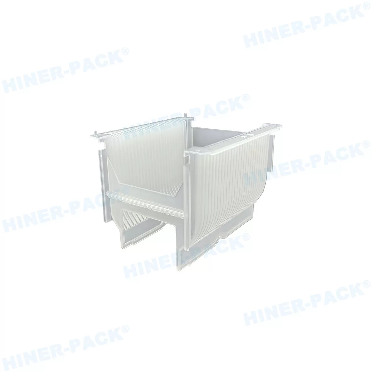
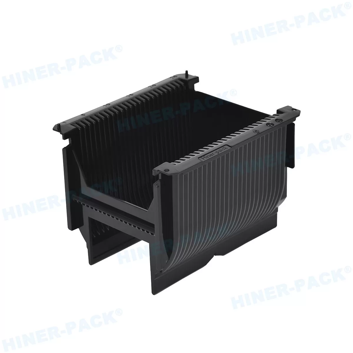
An industrial wafer holder manufacturer engineers far more than static plastic trays—it designs precision substrate retention systems that mitigate thin-wafer warpage, absorb transport vibration, and eliminate airborne molecular contamination (AMC) across automated Fab front-ends and OSAT packaging lines. Founded in 2013, Hiner-pack integrates product engineering, polymer R&D, in-house precision mold tooling, cleanroom injection, and global sales. Holding over 2,000 active mold assets and partnering with top-tier university material laboratories, Hiner-pack provides turnkey OEM/ODM single-wafer shippers, multi-slot process cassettes, and flex-frame carriers engineered to protect front-end silicon, compound SiC/GaN, and thinned die substrates.
Direct Factory Audit Standard (Short Answer)
A qualified wafer holder manufacturer must demonstrate four verifiable core competencies: sub-0.05 mm slot pitch registration, certified permanent polymer ESD networks (106–109 Ω/sq), low-outgassing resin compounding compliant with ASTM E595, and automated ISO Class 4 cleanroom DI water processing. Hiner-pack bypasses broker markups and eliminates upfront NRE mold costs by leveraging over 2,000 pre-existing toolsets, delivering direct factory pricing, 3-to-7-day rapid sampling, and drop-in SEMI mechanical compatibility for global fabs.
■ Key Sourcing Decisions at a Glance
Zero-NRE Tooling Asset
2,000+ existing molds eliminate upfront NRE fees for 100mm, 150mm, 200mm, and 300mm handling fixtures.
1. Mechanical Mechanics: Managing Thin-Wafer Warpage and High-Speed Robotics
As semiconductor wafers thin down to 50 micrometers or transition to highly stressed compound substrates (SiC/GaN), gravitational and thermal bowing causes severe edge drop-off. A precision wafer holder manufacturer must design slot geometries that cradle warped substrates without edge pinch-stress or end-effector transfer failure.
In modern automated fabs, Equipment Front End Modules (EFEM) rely on optical sensors and vacuum end-effectors to load wafers at rapid cycle rates. If a wafer holder experiences internal molding stress, the sidewalls subtly deflect inward under thermal cycling. This causes slot pitch variance, resulting in robotic arms scraping the active die surface or triggering emergency shut-offs.
Manufactured on uncalibrated manual injection presses. Wall thickness varies by >0.1 mm, causing uneven thermal shrinkage. Slots lack lead-in radiuses, inducing micro-fractures along the fragile wafer bevel during robotic insertion.
The Hiner-pack Solution
Engineered Precision Geometry
Molded on all-electric high-tonnage presses using mirror-EDM core inserts. Multi-angle guide pockets support bowed substrates with zero friction, while continuous CMM scanning certifies slot pitch parallelism within ±0.05 mm.
2. Advanced Polymer Compounding: Permanent ESD and Zero Chemical Outgassing
Semiconductor yield losses stem predominantly from two microscopic vectors: electrostatic discharge (ESD) and airborne molecular contamination (AMC). Hiner-pack operates an in-house polymer R&D base in partnership with domestic universities, synthesizing proprietary conductive compounds that guarantee permanent static dissipation without particulate shedding.
Low-tier plastic carriers frequently utilize temporary anti-static surfactants sprayed onto the surface. These topical coatings degrade rapidly, wash off in cleanroom DI water baths, and outgas volatile organic compounds (VOCs) that condense onto exposed copper interconnects. Other manufacturers load standard polymers with excessive raw carbon powder, which sloughs off under friction to create catastrophic conductive particle clouds.
Matrix-Dispersed Carbon Nanotubes & Conductive Polymers: Permanent volume resistivity locked at 106 to 109 Ω/sq. Non-migrating, humidity-independent, and completely carbon-shed-free.
Ultra-Low Outgassing PEEK, PFA, and PES: Vacuum-treated resins engineered for zero condensable volatile material (CVCM < 0.1%), preventing photo-acid generator poisoning in advanced lithography.
Ionic Purity Testing via ICP-MS: Strict batch screening ensures that trace mobile metal ions (Na+, K+, Fe2+, Cu2+) remain below detectable parts-per-billion (ppb) thresholds.
3. Tooling Scale: How 2,000+ Molds Protect Your Capex and Compressed Schedules
Developing custom injection molds for semiconductor carriers introduces severe friction: $5,000 to $20,000 in Non-Recurring Engineering (NRE) fees and 8 to 12 weeks of tooling lead time. Hiner-pack eliminates this barrier through an existing catalog of over 2,000 active mold toolsets, enabling immediate mass production.
Whether sourcing standard SEMI cassettes, horizontal transfer boats for diffusion furnaces, or high-security shipping jars for bumped die, our 2,000+ mold library allows global procurement managers to bypass tooling investments entirely. In over 85% of custom inquiries, our engineers map customer drawings directly to an active modular mold base.
2,000+Active Mold Sets
$0 NREOn Matched Tooling
72 HoursSample Dispatch Time
2–3 WeeksCustom Mold Lead Time
4. Engineering Sourcing Guide: Do's and Don'ts for Wafer Holder Procurement
PASSMandatory Engineering Checks (DO)
Audit existing mold availability: Check Hiner-pack's 2,000+ mold database to absorb specs without incurring NRE fees.
Mandate CMM coordinate verification: Confirm H-bar flatness, robotic pocket alignment, and slot run-out within ±0.05 mm.
Verify certified cleanroom cleaning: Require carriers washed with hot 18.2 MΩ·cm DI water inside verified ISO 14644-1 cleanrooms.
Specify core resin conductivity: Require multi-point resistivity data confirming volume dissipation without topical sprays.
FAILProcurement Red Flags (DON'T)
Don't source from trading brokers: Non-manufacturing agents lack cleanrooms, cannot modify mold tooling, and cannot trace resin batches.
Don't accept commercial plastic wrapping: Standard polyethylene bags generate massive static voltages and deposit particles directly onto carriers.
Don't overlook chemical compatibility: State your exact process acids (HF, H2SO4, RCA) to avoid sudden polymer embrittlement.
Don't buy on unit price alone: A wafer holder that drops a single 300mm patterned wafer will cost 100x its purchase price in lost yield.
5. The Hiner-pack Closed-Loop Lot Acceptance Framework
To ensure that every carrier batch integrates seamlessly into automated handling lines without mechanical friction or contamination, Hiner-pack executes a strict 5-phase quality proof pack on all production lots prior to shipment release.
Q1: How does Hiner-pack eliminate NRE mold costs for custom-dimension wafer holders?
A1: Established in 2013, Hiner-pack has accumulated an active asset library of over 2,000 mold toolsets. By utilizing modular mold bases with interchangeable pocket inserts, we can configure non-standard wafer pitch spacings, custom pocket depths, or specialized robotic lift profiles without machining entirely new mold blocks. This eliminates NRE tooling fees ($0 tooling charges) on the vast majority of customer inquiries.
Q2: Can Hiner-pack manufacture wafer holders for thinned and bowed compound wafers?
A2: Yes. We specialize in carriers for thinned silicon down to 50µm, compound Silicon Carbide (SiC), and Gallium Nitride (GaN) substrates. Our engineers design specialized lead-in pocket geometries with gentle perimeter ramp angles that cradle bowed wafers, preventing micro-fractures along edge bevels and eliminating robotic transfer clamping jams.
Q3: How is ESD protection permanently guaranteed across Hiner-pack carriers?
A3: We do not use temporary topical surfactant sprays. Supported by our joint university polymer R&D laboratory, Hiner-pack blends conductive carbon networks and inherently dissipative polymers directly into the base resin matrix (PEEK, PFA, PP, PC). This guarantees permanent surface and volume resistivity (106 to 109 Ω/sq) that survives aggressive acid immersion and ultrasonic cleaning without carbon particle shedding.
Q4: Can Hiner-pack wafer holders be introduced directly into fab cleanrooms?
A4: Yes. All Hiner-pack products pass through our in-house automated cleanroom cleaning lines. After multi-stage ultrasonic scrubbing and an 18.2 MΩ·cm hot DI water cascade rinse, products are baked dry and double vacuum heat-sealed inside certified ISO Class 4/5 cleanrooms using antistatic, outgassing-free barrier films. They require zero secondary on-site cleaning upon arrival.
Q5: What is the sample dispatch and mass-production lead time at Hiner-pack?
A5: For configurations matching our 2,000+ mold inventory, qualification samples ship within 72 hours (3 business days). Custom OEM/ODM designs requiring proprietary polymer compounding or in-house EDM mold insert tooling typically deliver certified first-article samples within 2 to 3 weeks, accompanied by full CMM coordinate metrology reports.
Q6: How does Hiner-pack support global logistics and distributor partnerships?
A6: Hiner-pack ships directly to leading semiconductor manufacturing hubs across North America, Europe, Taiwan, Japan, South Korea, and Southeast Asia. We provide export-grade vacuum crating, global freight terms (DAP, DDP, FOB), and offer factory-direct wholesale pricing to authorized international semiconductor packaging distributors.
Direct Wafer Holder Manufacturer · 2000+ Mold Library
Partner With Hiner-pack: Request Your Factory Specification Review
Ready to eliminate middleman markups, waive NRE tooling costs, and secure SEMI-compliant, cleanroom-ready wafer carriers? Leverage Hiner-pack’s decade-long manufacturing expertise, in-house polymer R&D labs, and extensive 2,000+ mold library today.
✓ 2000+ Active Mold Sets✓ In-House Polymer R&D✓ ISO Class 4 Cleanroom✓ Manufacturer-Direct Pricing