Stay Informed with Hiner-pack’s Latest Developments
Home>Blog>
Top 10 Wafer Holder Suppliers for Safe Semiconductor Packaging in 2026
Top 10 Wafer Holder Suppliers for Safe Semiconductor Packaging in 2026
2026-09-18
Wafer fabrication and advanced packaging tolerances are tighter than ever. As
the semiconductor industry moves deeper into 2026, trends like Chiplet
architectures, 3D heterogeneous integration, and compound semiconductors (SiC
and GaN) demand extreme mechanical precision. At the same time, wafers ground
down to double-digit micrometer profiles warp easily under minimal mechanical
stress.
In this high-stakes production environment, a wafer carrier is not merely a
transport box. It is an active safeguard for front-end and back-end device
yields. A single micro-scratch, an electrostatic discharge (ESD) spark, or trace
chemical outgassing can ruin an entire production lot. Finding a qualified wafer
holder supplier has therefore shifted from a routine purchasing task to a
strategic engineering decision. Specialized manufacturers like Hiner-pack and
global legacy brands are continually upgrading their material science and
tooling capabilities to meet these cleanroom demands.
This guide analyzes the market dynamics, outlines essential carrier selection
metrics, and ranks the top 10 wafer holder suppliers capable of securing your
wafer transport lines in 2026.
Packaging engineers and procurement managers must evaluate several technical
benchmarks before signing an annual supply contract with any wafer holder
supplier. We used five objective criteria to select the vendors featured in this
guide:
Polymer Engineering and ESD Control: Does the supplier
formulate proprietary polymers? Carriers must maintain surface resistivities
between 105 and 109 ohms/sq without carbon sloughing.
Materials like high-purity Polypropylene (PP), Polyetheretherketone (PEEK), and
Polyethersulfone (PES) must exhibit near-zero ionic contamination and ultra-low
outgassing.
Cleanroom Processing and Washing Lines:Wafer carriers must
not generate particulate matter. Top manufacturers maintain ISO Class 4 (Class
10) or ISO Class 5 (Class 100) cleanrooms for precision injection molding,
ultrasonic deionized water cleaning, and vacuum packaging.
Shock Absorption and Mechanical Restraint: Thin wafers flex
under vibration during freight transport. Carriers require dynamic perimeter
suspensions, precision wafer slots, and shock-dampening cushions that prevent
wafer edge-chipping and lateral movement.
Tooling Depth and OEM/ODM Capability: Custom silicon
geometries, thick substrates, and specialized frames require custom tooling.
Suppliers with large libraries of existing molds save clients months of tooling
lead times and tens of thousands of dollars in non-recurring engineering (NRE)
fees.
Total Cost of Ownership and Sustainability: Modern
semiconductor fabs demand reusable, chemically resilient cassettes and coin
boxes that survive hundreds of cleaning cycles, lowering the cost per transit
cycle.
Founded in 2013, Hiner-pack has developed into a full-scale high-tech
manufacturer specializing in IC packaging materials, wafer handling cassettes,
automated carrier systems, and protective transit boxes. The company operates as
a direct manufacturer, providing turnkey custom solutions that bridge the gap
between front-end silicon fabrication and OSAT operations.
Hiner-pack maintains an internal polymer engineering unit partnered with
academic research institutes. This technical focus has yielded proprietary
antistatic compounds that demonstrate virtually zero outgassing and high
mechanical rigidity. Their custom polymer blends prevent particle shedding
during high-speed automated picking, making them suitable for sensitive 200mm
and 300mm wafer transfer processes.
One of Hiner-pack's strongest competitive advantages is its tooling
inventory. With more than 2,000 existing molds available, the company supports
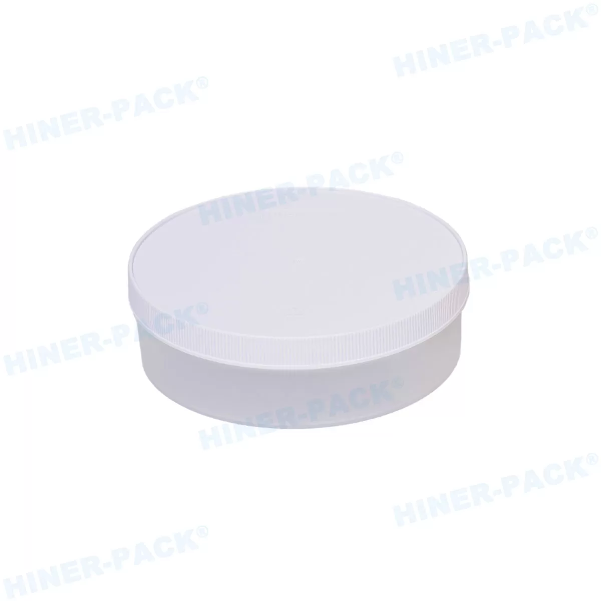
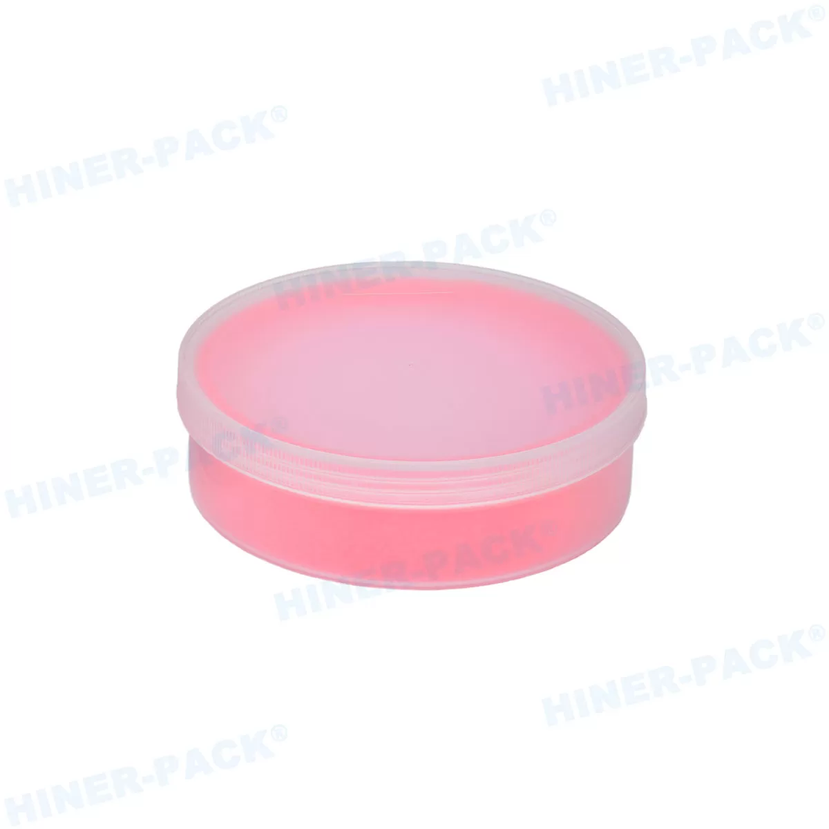
standard silicon wafers, thin-film substrates, diced ring frames, coin-style
boxes, and specialized wafer jars without requiring costly new mold builds.
Their precision tooling workshop and automated injection molding lines are
backed by Class 100/1000 cleanroom washing facilities.
For operations aiming to reduce bill-of-materials overhead without
sacrificing cleanliness or physical protection, Hiner-pack provides flexible
OEM/ODM capabilities. Backed by extensive patent holdings in structural carrier
designs, the company supplies fabs worldwide and is actively expanding its
network of global distributors.
2. Entegris
Headquartered in the United States, Entegris remains a long-standing
standard-setter for advanced front-end materials handling. Their Front Opening
Unified Pods (FOUPs) and Front Opening Shipping Boxes (FOSBs) dominate Tier-1
300mm automated fabs. While their technological capability and contamination
control are proven, their products carry significant price premiums and extended
delivery schedules.
3. Shin-Etsu Polymer
As a subsidiary of Japan's Shin-Etsu Chemical, Shin-Etsu Polymer excels in
raw polymer synthesis and ultra-clean wafer shipping containers. Their products
are widely specified for bare silicon shipping from primary wafer manufacturers
to processing fabs. Their material purity is among the highest in the industry,
supported by decades of specialized chemical production.
4. Miraial
Miraial is a Japanese precision equipment company recognized for its
high-performance resin manufacturing. They specialize in cassettes, processing
boats, and shippers using high-grade fluoropolymers (such as PFA). Miraial
carriers are built for aggressive wet-bench chemical baths, acidic cleaning
processes, and harsh thermal operations.
5. Gudeng Precision
Based in Taiwan, Gudeng Precision is a critical partner in the advanced
lithography and packaging supply chain. Best known for EUV pod innovations,
Gudeng also manufactures high-end wafer cassettes and automated carriers
tailored to leading-edge foundries. Their designs are optimized for automated
material handling systems (AMHS).
6. Brooks Automation
Brooks Automation approaches wafer carriers through an automation-first lens.
Based in the United States, Brooks manufactures automated wafer transfer
modules, storage reticle systems, and integrated carriers. Their solutions cater
to fabs looking to eliminate manual operator interventions across their wafer
handling footprint.
7. 3M Semiconductor Solutions
3M provides essential wafer packaging and transport consumables, notably
precision conductive carrier tapes, wafer protective tapes, and antistatic
cushioning pads. While not an injection molder of large FOUP systems, 3M remains
an indispensable supplier for wafer-level packaging and dice-transit
applications.
8. E&R Engineering
Taiwan-based E&R Engineering supplies the semiconductor assembly,
packaging, and testing sectors. Beyond their laser systems and automation
machinery, they produce specialized carrier cassettes and processing boats
engineered for OSAT strip and wafer sorting operations.
9. Pozzetta
Headquartered in the United States, Pozzetta manufactures secure transport
carriers for photomasks, reticles, and silicon wafers. They specialize in
high-integrity packaging enclosures that eliminate micro-movement during air
transport, protecting sensitive substrates from transit-induced mechanical
damage.
10. DAINICHI SHOJI
DAINICHI SHOJI is a veteran Japanese supplier of wafer cassettes, storage
cabinets, and chemical-handling containers. Their carriers are recognized for
mechanical stability across high-temperature cleaning regimes, serving both
mainstream silicon and compound semiconductor fabs.
Wafer Holder Buyer’s Guide for 2026
Choosing the correct wafer carrier requires matching product specifications
to distinct manufacturing environments. Procuring front-end fab carriers
involves different criteria than outfitting high-volume OSAT back-end packing
lines.
Front-End Fab vs. Back-End OSAT Handling Requirements
Front-end fabs prioritize zero chemical outgassing and particle prevention
down to single-digit nanometer levels. These processes require expensive
materials like virgin PFA, PES, or specialized polycarbonate. In contrast, OSAT
facilities and wafer shipping operations focus on physical impact dampening,
broad chemical resistance against post-dicing wash agents, reliable ESD
dissipation, and cost per carrier.
Using high-priced front-end FOUPs for inter-facility shipping increases
packaging budgets unnecessarily. A reliable wafer holder supplier like
Hiner-pack can provide antistatic conductive PP carriers that deliver identical
mechanical protection and static mitigation for back-end transit at a fraction
of the cost.
The Advantage of Factory-Direct Manufacturers with In-House Molds
Mid-tier distributors and trading firms often face severe supply chain
bottlenecks. Working directly with a primary tooler and molder provides several
operational advantages:
Reduced Lead Times: Suppliers with extensive pre-existing
tooling libraries (such as Hiner-pack's 2,000+ mold inventory) can begin
production immediately, cutting setup periods from months down to days.
Tailored Form Factors: Standard silicon sizes (100mm,
150mm, 200mm, 300mm) are straightforward, but thinned wafers, glass carriers, or
reconstituted panel rings require custom internal rib profiles. Factory-direct
engineering teams adjust mold inserts without red tape.
Price Predictability: Direct raw material compounding and
in-house molding remove intermediary markups, protecting margins against supply
chain swings.
Cleanliness and Compliance Verification Checklist
Before qualifying a new supplier, request third-party lab documentation
verifying the following industry standards:
ANSI/ESD S20.20 Certification: Ensures reliable surface
resistivity and controlled charge decay times without hot spots.
Liquid Particle Counting (LPC): Validates that carrier
surfaces release negligible sub-micron particulates during fluid agitation.
Airborne Particle Counting (APC): Verifies that cleanroom
packaging facilities maintain their designated ISO Class rating.
RoHS and REACH Compliance: Guarantees that flame
retardants, plasticizers, and stabilizers contain no restricted heavy metals or
hazardous chemicals.
Frequently Asked Questions
Q1: What materials are best for safe semiconductor wafer
holders? A1: The optimal material depends on the operating
environment. For general transport and back-end OSAT protection, carbon-loaded
or inherently dissipative conductive Polypropylene (PP) provides the best
balance of impact resistance, ESD safety, and cost efficiency. For
high-temperature wet benches or chemical processing, fluoropolymers like PFA or
high-end engineering polymers like PEEK and PES are preferred because of their
heat deflection ratings and acid resistance.
Q2: How do wafer holders prevent static damage (ESD) during
transport? A2: Quality wafer holders use conductive or
static-dissipative polymer additives compounded directly into the resin matrix.
This delivers a controlled surface resistivity (typically 105 to
109 ohms per square). As a result, static charges bleed off gradually
to ground rather than discharging suddenly into the microchips, preventing gate
oxide breakdowns and latent junction damage.
Q3: Why choose an OEM/ODM wafer carrier supplier over a traditional
brand distributor? A3: Traditional distributors sell fixed catalog
products with high markups and rigid minimum order volumes. Direct OEM/ODM
manufacturers like Hiner-pack can alter slot pitches, modify internal wafer
retaining springs, and adjust material hardness to match your exact substrate
thickness. This eliminates custom re-tooling costs while providing direct access
to the team manufacturing your components.
Q4: Can wafer shipping boxes and cassettes be reused across multiple
transit cycles? A4: Yes, provided they are made from structurally
resilient polymers and maintained properly. Rigid wafer jars, coin boxes, and
cassettes can be collected, routed through automated deionized water ultrasonic
wash systems, dried in cleanrooms, and inspected for reuse. This multi-trip
lifecycle approach significantly reduces single-use plastic waste and lowers
unit packaging costs.
Q5: What packaging design features best protect ultra-thin wafers
from cracking? A5: Ultra-thin wafers (under 100 micrometers) are
vulnerable to edge-chipping and flexural fatigue. Safe carriers use contoured
perimeter cushions, spider springs that distribute clamping force evenly along
wafer edges, and precision-machined guide slots that restrict vertical movement
without applying direct pressure to active die areas.
Secure Your Semiconductor Supply Chain Today
The advanced packaging roadmap for 2026 allows zero room for handling-induced
yield loss. Selecting the right wafer holder supplier safeguards your silicon
assets against transit shock, electrostatic failure, and cleanroom particulate
contamination. Relying on suppliers that combine custom polymer engineering with
deep mold inventories provides both technical safety and cost advantages.
Are you looking to optimize your wafer handling systems, reduce component
packaging overhead, or explore high-margin distributor opportunities? Contact
the engineering team at Hiner-pack today to request your 2026
Product Catalog, review mold compatibility sheets, and arrange free sample
carrier evaluations for your cleanroom line.