
For semiconductor fab managers, OSAT procurement specialists, and packaging engineers, budgeting for component carriers involves a delicate balance: controlling operational expenses while eliminating the catastrophic yield risks of static discharge, outgassing, and mechanical shock. When analyzing the wafer trays price in the global market, quotes can range anywhere from under $2.00 for standard coin shippers to well over $50.00 for precision, high-temperature, cleanroom-baked carriers.
Why is there such a broad pricing spread? What technical variables truly dictate the cost of a semiconductor carrier? This guide breaks down the core engineering drivers behind wafer carrier pricing and outlines how partnering directly with a turnkey manufacturer like Hiner-pack provides direct factory savings without sacrificing component integrity.
Looking for immediate volume pricing? Contact Hiner-pack for a Factory-Direct Quote & Free Evaluation Samples.
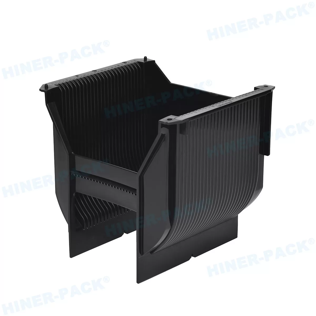
1. The 4 Engineering Drivers That Determine Wafer Trays Price
The price of a wafer tray or carrier is never arbitrary. It is governed by four primary engineering and manufacturing cost drivers:
Polymer Compounding & Raw Material Grade: Standard commercial plastics are inexpensive but lack static dissipation. Inherently conductive polymers compounded with carbon networks or advanced polymers like PEEK and PES require specialized compounding, directly influencing the baseline raw material cost.
Mold Tooling Precision & Cavity Complexity: High-precision injection molds machined via CNC and EDM to sub-micron tolerances carry upfront tooling investments, but ensure zero burrs, uniform wall thickness, and precise robotic automation alignment.
Cleanroom Processing & Washing Standards: Manufacturing inside an ISO-certified cleanroom, combined with multi-stage ultrasonic deionized (DI) water washing and double-vacuum packaging, adds processing value by ensuring zero particulate contamination upon delivery.
Testing & Compliance Certification: Reliable suppliers verify every batch using surface resistivity meters, optical coordinate measuring machines (CMM), and outgassing analysis to provide certified quality documentation.
2. Material Grade vs. Price & Performance Matrix
The selection of raw materials is the single largest variable in determining the unit price of wafer trays. Below is an engineering comparison of typical material classifications, performance parameters, and relative cost profiles:
| Material Classification | Surface Resistivity (Ω/sq) | Thermal Tolerance | Relative Price Level | Primary Semiconductor Application |
|---|---|---|---|---|
| Standard Natural PP / PS | Insulative (>10^12) | Up to 60°C | Low ($) | Non-sensitive substrate storage, basic mechanical protection |
| Conductive PP (Black) | 10^4 - 10^6 (Permanent) | ~80°C | Moderate ($$) | Fab-to-fab transit, standard wafer shipping (2" to 12") |
| Static Dissipative Engineered Resins | 10^6 - 10^9 (Clean ESD) | 80°C - 120°C | Moderate to High ($$$) | Automated sorting, pick-and-place lines, low-particle packaging |
| High-Temp Modified PEEK / PES | 10^6 - 10^9 (Bakeable) | 150°C - 200°C+ | Premium ($$$$) | In-tray baking, vacuum degassing, high-temperature test processes |
3. Off-the-Shelf Catalog Trays vs. Custom Tooling Costs
When calculating total procurement expenditure, buyers must choose between standard catalog items and custom-engineered molds:
Standard Catalog Carriers (Zero Tooling Investment)
If your application uses industry-standard 2", 4", 6", 8", or 12" wafers, standard single-wafer shippers, coin boxes, and multi-wafer cassettes provide the lowest overall wafer trays price because mold development costs are already amortized by the manufacturer.
Custom OEM/ODM Tooling (Bespoke Geometry)
For custom die sizes, optical sensors, microfluidic chips, or specialized GaN/SiC substrates, custom molds are required. Tooling investments (NRE) typically range from $1,500 to $8,000+ depending on pocket complexity and mold cavitation. However, custom tooling eliminates carrier rattling, reduces scrap rates, and lowers the long-term unit cost for mass production.
4. How Hiner-pack Delivers Factory-Direct Cost Advantages
Founded in 2013 in Shenzhen, China, Hiner-pack is an integrated high-tech enterprise integrating R&D, mold manufacturing, and cleanroom injection molding. We help customers optimize their supply chain costs through key structural advantages:
In-House Material Compounding: Developed in cooperation with university polymer research institutes, our proprietary ESD and high-temperature formulations reduce raw material costs compared to third-party compounded plastics.
Direct Manufacturer Pricing: By eliminating distributor markups, trading company margins, and overseas handling fees, you receive direct factory pricing.
Integrated Tooling & Production: We manage mold design, CNC fabrication, and high-speed injection under one roof, reducing lead times and prototyping expenses.
Comprehensive Product Catalog: One-stop sourcing for Wafer Carriers, Shipper Accessories (sponges, separator sheets), JEDEC Trays, Waffle Packs, and Gel Boxes reduces consolidation and international shipping overhead.
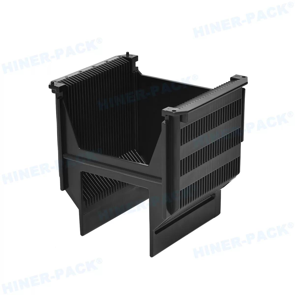
Engineering Verification: Free Samples & Pricing Quotation
Ensure your packaging meets both your technical specifications and budget targets before committing to volume production.
What Your Pricing & Evaluation Package Includes:
Tiered Volume Quotation: Transparent unit pricing broken down by batch sizes (prototyping, 500 pcs, 2,000 pcs, 10,000+ pcs).
Free Qualification Samples: Functional sample trays provided for dimensional check, automated handler testing, and drop tests.
Complete Material Datasheet: Detailed ESD resistance curves, outgassing data, and thermal compliance certificates.
Tooling Feasibility Review: Free DFM (Design for Manufacturability) analysis for custom carrier designs.
How to Request Your Custom Quotation:
Submit Your Parameters: Email your required wafer size, material preference (Conductive PP, Bakeable, etc.), and estimated annual quantity.
Receive Fast Engineering Feedback: Our technical team provides a detailed quotation and CAD verification within 24 hours.
Sample Testing: Receive cleanroom-packed evaluation samples within 48 hours for immediate fab qualification.
Direct Inquiries: Contact our pricing team at rainbowzhu@hiner-pack.comfor immediate project support.
Frequently Asked Questions About Wafer Trays Price
Q1: What is the typical wafer trays price range for standard semiconductor carriers?
A1: Standard single-wafer shippers and coin-style boxes in conductive PP generally range from $1.50 to $6.00 per unit depending on diameter (2-inch vs. 12-inch) and order volume. Multi-wafer cassettes and high-temperature bakeable JEDEC trays typically range from $8.00 to $35.00+ due to the higher volume of engineered resin (such as PEEK or modified PES) and strict dimensional tolerances.
Q2: How can semiconductor procurement teams lower their overall wafer trays price?
A2: Sourcing directly from an integrated injection molder like Hiner-pack is the most effective way to reduce costs. Additionally, consolidating orders across multiple packaging formats (e.g., combining wafer shippers, separator cushions, and waffle packs in one shipment) reduces freight expenses, while standardizing material requirements helps take advantage of higher volume resin discounts.
Q3: How much does custom mold tooling cost for a proprietary wafer or chip tray?
A3: Custom tooling costs vary depending on tray complexity, pocket count, and required mold steel grade. Standard precision single-cavity prototype tooling typically starts around $1,500 - $3,000, while high-volume multi-cavity automated production molds range from $4,000 to $8,000+. Hiner-pack frequently offers tooling rebate programs where mold costs are credited back once mass production volumes reach agreed thresholds.
Q4: Does a lower wafer trays price imply higher yield risks during shipping?
A4: Not necessarily, provided the carrier is purchased directly from a certified manufacturer rather than a low-grade generic supplier. Cost reductions should come from efficient tooling, in-house polymer compounding, and automated injection molding—never from using non-permanent antistatic sprays, recycled contaminated regrind, or uncalibrated injection molds.
Ready to optimize your semiconductor packaging budget? Send your specifications directly to our engineering team at rainbowzhu@hiner-pack.com to receive your factory-direct quote today.














