
In modern semiconductor manufacturing, protecting microelectronic substrates during transport and processing is paramount to maintaining high yield rates. As fabrication facilities migrate to smaller process nodes, the tolerance for particulate contamination, chemical outgassing, and electrostatic discharge decreases. This makes substrate protection packaging an active element of contamination control. When evaluating global supply chain logistics, understanding the variables that dictate the wafer container price is a priority for fabrication facilities, assembly operations, and material procurement departments.
The acquisition of high-purity shipping and process carriers involves balancing mechanical specifications with budgetary constraints. Industry suppliers like Hiner-pack provide specialized engineering solutions that balance cleanroom performance with cost-efficiency. This analysis explores the material choices, regulatory standards, and mechanical configurations that influence pricing in the global semiconductor marketplace.
Categorizing Wafer Carriers: Functional Designs and Sourcing Tiers
The physical structure of a carrier is the primary driver of its manufacturing cost. Different processing phases require distinct levels of isolation, which dictates the complexity of the carrier design.
Front Opening Unified Pods (FOUPs)
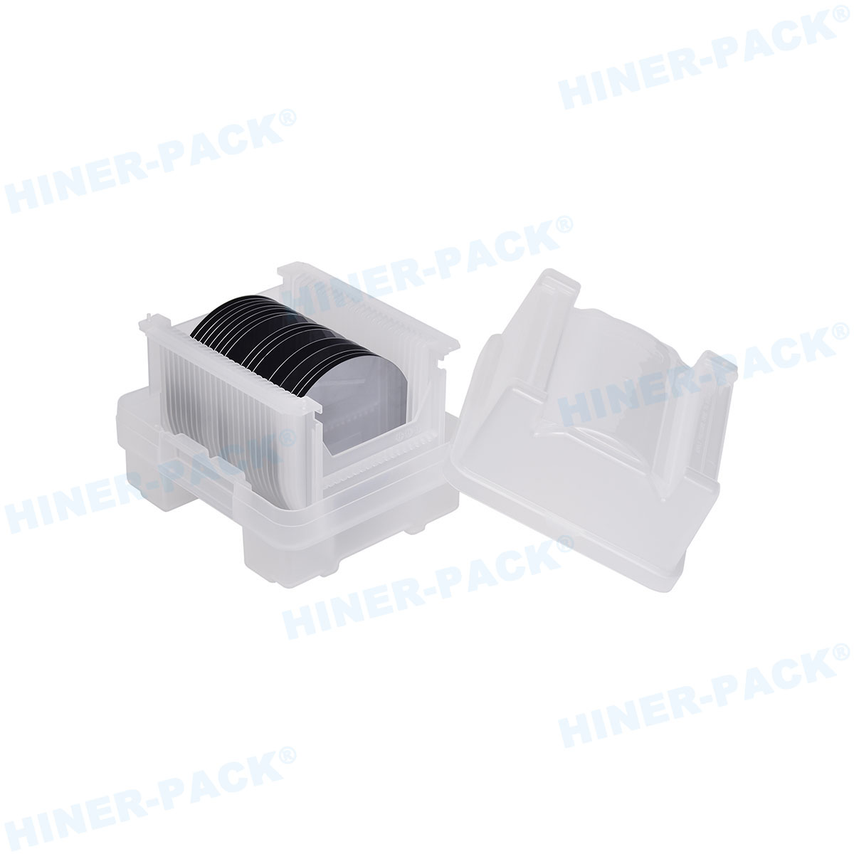
Designed primarily for 300mm wafer fabrication facilities, Front Opening Unified Pods represent the highest tier of substrate enclosure. These systems protect wafers from ambient cleanroom air by maintaining an isolated, controlled internal microenvironment. FOUPs interface directly with automated material handling systems (AMHS) and tool load ports. The integration of precise registration features, robotic lifting flanges, and complex door-opening mechanisms contributes to their higher pricing. The precision molding and tight tolerances required for seamless tool integration make these carriers the most significant investment in the wafer transport category.
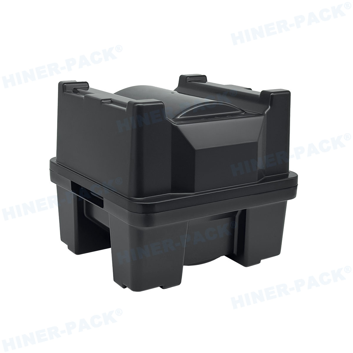
Front Opening Shipping Boxes (FOSBs)
While FOUPs are optimized for internal fab automation, Front Opening Shipping Boxes are engineered for inter-facility transport. They feature robust latching mechanisms and vibration-dampening internal supports to protect wafers during air and overland shipping. Although they do not require the continuous automation interface capabilities of a FOUP, their structural integrity and sealing performance must withstand pressure differentials and impact during shipping. Consequently, their pricing reflects these heavy-duty mechanical requirements.
Open Cassettes and Horizontal Wafer Shippers
For smaller wafer diameters (such as 150mm and 200mm) and legacy manufacturing lines, open cassettes and horizontal shippers are widely utilized.
Open Cassettes: These allow direct exposure to cleanroom environments and are designed for wet chemistry, thermal processing, or transport within manual fabs. Their simpler design makes them more economical.
Horizontal Shippers and Coin Stacks: Used primarily for shipping raw, unpatterned wafers or finished dies, these configurations secure wafers in a compact stack, often utilizing protective liners. They offer a cost-effective option for transport when automated tool compatibility is not required.
The structural differences between these formats directly explain the variance in the wafer container price across the industry.
Material Science: How Polymers Dictate Cost and Performance
The selection of plastic resins and additives directly affects both the physical performance of a carrier and its raw material costs. Semiconductor-grade polymers must exhibit exceptional dimensional stability, high purity, low outgassing properties, and static dissipation.
Polycarbonate (PC)
Polycarbonate is the standard material for many shipping boxes and standard cassettes. It offers excellent impact resistance, high dimensional stability, and transparency, allowing for visual inspection of the wafers inside. For less demanding environments or standard shipping operations, polycarbonate provides a dependable balance of physical protection and reasonable procurement costs.
Polyetheretherketone (PEEK)
For high-temperature processing, chemical exposure, and ultra-low outgassing requirements, Polyetheretherketone (PEEK) is the industry standard. PEEK resists thermal deformation and chemical degradation from aggressive solvents and acids. However, the raw material cost of PEEK is substantially higher than that of standard polycarbonates, which is reflected in the final pricing of carriers manufactured from this polymer.
Cyclic Olefin Copolymer (COP)
Commonly specified for FOUP shells, COP offers low moisture absorption and excellent barrier properties against airborne molecular contamination (AMC). Its high transparency and chemical purity make it ideal for monitoring wafer status in advanced nodes. Due to its advanced synthesis process, COP is positioned as a premium material option.
Carbon-Fiber Reinforcement and ESD Additives
Unmodified polymers are naturally insulative and can accumulate static charge, which attracts airborne particles and causes electrostatic discharge (ESD) events that ruin integrated circuits. To mitigate this, polymers are compounded with conductive carbon powder, carbon fibers, or inherently dissipative polymers (IDPs). The integration of these additives is necessary to control surface resistivity (typically between 10^5 and 10^11 ohms/sq). The inclusion of high-purity conductive fillers increases the complexity of the compounding process, impacting the raw material costs.
| Material Class | Key Structural Properties | Primary Application Areas | Relative Cost Bracket |
|---|---|---|---|
| Polypropylene (PP) | Flexible, cost-effective, chemical resistance | Coin stacks, low-cost transport | Economy |
| Polycarbonate (PC) | Transparent, rigid, high impact strength | Standard shipping boxes, FOSB shells | Moderate |
| Cyclic Olefin Copolymer (COP) | Ultra-low outgassing, high purity, low moisture | Advanced FOUP shells, process carriers | High |
| PEEK (Carbon-Filled) | Extreme thermal stability, high wear resistance | Process cassettes, high-reliability FOUP components | Premium |
Specifying high-performance polymers for demanding processes inevitably affects the wafer container price. Sourcing professionals must evaluate whether their processing environments require premium materials or if standard polymers are sufficient.
Standards Compliance and Cleanroom Production Standards
The semiconductor industry relies on standardized dimensions and performance criteria to ensure global compatibility between different fabrication steps and equipment manufacturers.
SEMI Standards Compliance
Semiconductor Equipment and Materials International (SEMI) establishes strict guidelines for wafer carrier dimensions. Standard specifications like SEMI E47.1 (governing 300mm FOUPs) and SEMI E1.9 (governing mechanical interfaces) ensure that carriers fit seamlessly onto robotic load ports, end effectors, and storage buffers. Verifying compliance requires precise metrology testing and high-tolerance injection molding tools. The continuous calibration of these production systems is a major component of manufacturer overhead.
Cleanroom Manufacturing Environment
Because these carriers directly contact silicon wafers, they must be free of particulate contamination. This requires production, assembly, and packaging to occur within ISO Class 3 or Class 4 cleanroom environments.
Ultra-Pure Water Rinsing: Carriers undergo multi-stage wash cycles using deionized water to remove surface particles.
Vacuum Double-Bagging: Finished carriers are immediately sealed in multi-layer ESD-safe bags inside the cleanroom to prevent contamination during transit.
These labor-intensive verification processes are built directly into the final wafer container price. Leading packaging manufacturers, including Hiner-pack, implement rigorous quality control systems to ensure that every shipment arrives ready for cleanroom deployment.
Supply Chain Dynamics and Volume Sourcing Strategies
When planning packaging procurement, understanding manufacturing economics can help optimize procurement budgets.
Tooling Amortization and Production Volume
Developing high-precision injection molds for wafer carriers requires substantial initial capital. These molds must handle high pressures and temperatures while maintaining sub-millimeter tolerances over hundreds of thousands of cycles. For specialized designs with low production volumes, the cost of this tooling is amortized over a smaller run of units, leading to higher unit pricing. Conversely, high-volume orders for standard, widely compatible designs allow manufacturers to distribute tooling costs across larger production runs, lowering the unit price.
Customization and Purge Valve Integration
Modern advanced nodes often require controlled internal environments to prevent the oxidation of exposed metal layers on processed wafers. Integrating specialized features like nitrogen purge valves, smart tracking RFID tags, or custom slot pitches adds complexity to the carrier design. While these features improve process yield, they also increase production steps and cycle times, which raises the final cost of the carrier.
For standard processes, balancing design complexity against production volume is key to managing the overall wafer container price.
Navigating the Procurement Cycle: Request for Quote (RFQ) Protocols
To secure accurate and competitive pricing, procurement and engineering teams should provide detailed specifications during the RFQ process. This clear communication helps avoid delays and ensures the selected carrier aligns with fab requirements. Key details to include are:
Wafer Specifications: Indicate the precise wafer diameter (e.g., 100mm, 150mm, 200mm, or 300mm) and wafer thickness, as these determine the slot dimensions and carrier spacing.
Material Classification: Specify whether the carrier requires standard Polycarbonate, chemical-resistant Polypropylene, high-temperature PEEK, or carbon-filled ESD-safe compounding.
Process Compatibility: Define whether the carrier will be used for manual wet benches, high-temperature ovens, vacuum chambers, or automated AMHS tools.
Contamination Tolerances: Outline the required cleanroom packaging standards and permissible particulate and outgassing thresholds.
Order Volume and Schedule: State the initial order size and projected annual usage, as production volume directly influences manufacturing cost structures.
By submitting a structured RFQ, engineering teams can consult with Hiner-pack to align product specifications with production budgets.
Industry FAQs
Q1: Why does a 300mm FOUP have a much higher pricing structure than a standard 200mm open cassette?
A1: A 300mm FOUP is an enclosed microenvironment featuring robotic interface components, door sealing gaskets, registration coupling pins, and automated latching mechanisms. These complex parts require tight manufacturing tolerances to ensure compatibility with Fab load ports and AMHS systems. In contrast, an open 200mm cassette is a single-piece molded rack designed for manual handling or basic wet-bench processing, which requires fewer components and simpler manufacturing processes.
Q2: How do ESD-safe materials impact the pricing of wafer shipping boxes?
A2: ESD-safe materials require compounding base polymers with conductive additives, such as carbon fibers or carbon powder, to achieve a specific surface resistivity range. This compounding process requires extra manufacturing steps and precise quality control to ensure uniform conductivity. The cost of these high-purity additives and the associated testing protocols make ESD-safe containers more expensive than standard non-conductive plastic carriers.
Q3: Does the cleanroom ISO classification of the packaging facility affect the final product pricing?
A3: Yes. Operating and maintaining ISO Class 3 or Class 4 cleanrooms requires continuous air filtration, environmental monitoring, deionized water purification, and specialized protective gear for cleanroom staff. The manufacturing, cleaning, and multi-layer vacuum packaging of carriers within these controlled environments add operational overhead, which is reflected in the final cost of the carrier.
Q4: What role do nitrogen purge valves play in wafer container specifications and pricing?
A4: Nitrogen purge valves allow fabs to displace ambient air within the carrier with ultra-pure nitrogen gas, preventing wafer surface oxidation and moisture-induced contamination. Integrating these spring-loaded, leak-free valves requires extra manufacturing steps, precise alignment, and functional seal testing, which adds a premium to the cost of the carrier.
Q5: Can customized slot spacing or structural configurations be accommodated without a major price spike?
A5: Custom configurations usually require modifying injection molds or creating new tooling, which can carry significant upfront costs. However, some manufacturers utilize modular mold inserts that allow minor adjustments to slot depths or spacing without fabricating an entirely new mold core. Discussing your specific requirements early in the design phase can help identify the most cost-effective customization path.


