
The global semiconductor manufacturing pipeline demands strict control over ambient environments, mechanical vibration, and particulate contamination. As silicon wafers progress through front-end lithography and back-end packaging, their structural and chemical integrity remains highly susceptible to external variables. Selecting the appropriate transport and storage architecture is not merely a logistical consideration; it is a direct contributor to device yield. When packaging engineers and procurement managers prepare to secure a wafer container quotation, they must look beyond basic dimensions and analyze raw material properties, mechanical tolerances, and cleanliness standards. This analysis explores the precise parameters that dictate high-purity wafer carrier selection and how to structure procurement inquiries effectively.
The Engineering Fundamentals of Semiconductor Wafer Carriers
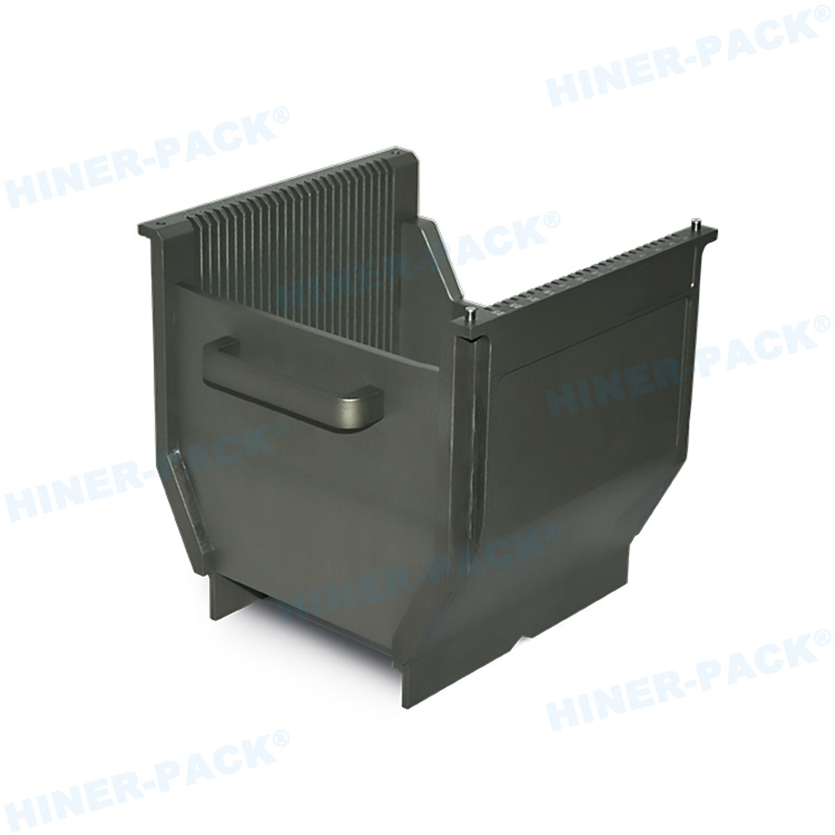
Modern microelectronics transport systems are complex micro-environments designed to preserve the surfaces of polished silicon, gallium nitride, or silicon carbide substrates. A standard plastic enclosure cannot provide the required shielding from ambient hazards. Consequently, specifying the correct mechanical attributes is the first step in obtaining a precise wafer container quotation from qualified manufacturers.
Polymer Chemistry and Outgassing Parameters
The chemical composition of a wafer carrier directly influences the yield safety of the micro-components inside. Standard industrial polymers often release volatile organic compounds (VOCs) over time, a process known as outgassing. In cleanroom environments, these airborne molecular contaminants (AMCs) can condense onto the wafer surface, leading to gate oxide breakdown or lithographic patterning defects. To prevent this, specialized materials are engineered for wafer transport:
Polycarbonate (PC): Highly favored for its dimensional stability, impact resistance, and optical clarity. It is commonly used for standard shipping boxes and automated material handling system (AMHS) interfaces.
Polyetheretherketone (PEEK): Selected for high-temperature applications, such as inline processing cassettes. PEEK offers exceptional chemical resistance and ultra-low outgassing profiles, though it carries a premium material cost.
Polybutylene Terephthalate (PBT): Provides high mechanical stiffness and resistance to chemicals used in wafer cleaning processes, making it ideal for process cassettes.
Polypropylene (PP): Typically utilized for low-cost horizontal shipping boxes or intermediate storage where high temperature resistance is not a primary concern.
Electrostatic Discharge (ESD) Protection
Electrostatic discharge represents a major hazard during dry cleanroom processing and transit. Triboelectric charging—the accumulation of static charge through friction—can occur when wafers slide inside carrier slots. If this charge discharges rapidly, it can destroy sub-micron circuitry. To mitigate this hazard, wafer containers are engineered with static-dissipative or conductive properties. Incorporating carbon powder or carbon fiber additives allows the material to achieve a surface resistivity in the static dissipative range (typically between 105 and 109 ohms per square). Specifying these electrical performance parameters is a vital step when preparing a request for a wafer container quotation.
Addressing Industry Logistics Challenges and Contamination Sources
The physical journey of a silicon wafer from raw ingot slicing to final packaging involves multiple physical transfers, often across different countries. During this journey, several vectors of potential yield degradation must be controlled through intelligent packaging design.
Particulate Management in Transit
Even inside a sealed container, micro-vibrations during shipping can cause the wafer edge to rub against the carrier slots. This friction generates microscopic particulate matter. If these particles settle on active die areas, they cause circuit opens or shorts. Advanced designs, such as those manufactured by Hiner-pack, utilize precision-molded structures with optimized slot profiles to secure wafers firmly. This minimizes lateral movement and limits the generation of micro-debris during long-distance air or road freight.
Mechanical Shock and Structural Ribbing
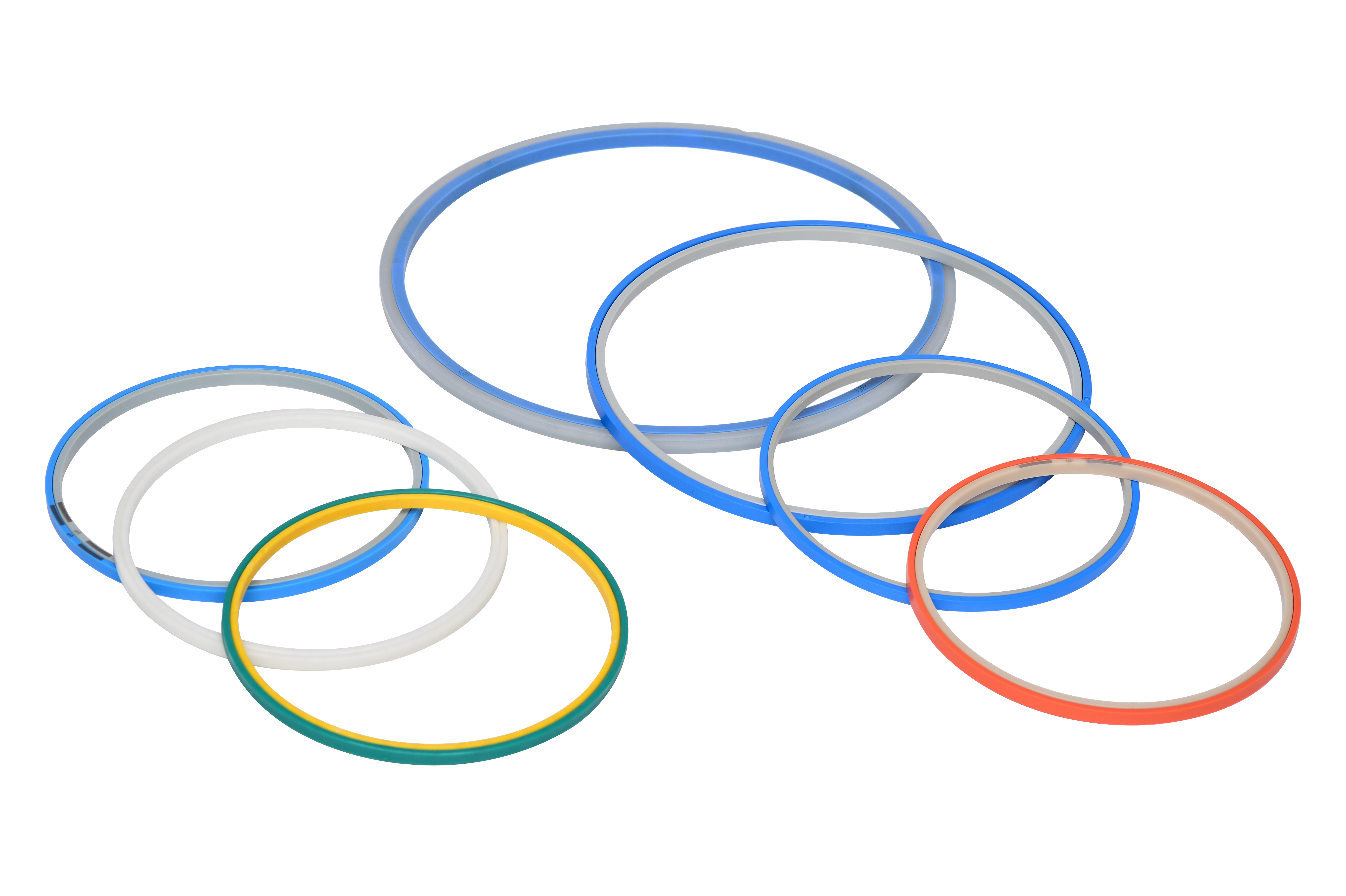
Shipping boxes must absorb external impacts without transferring kinetic energy directly to the fragile silicon inside. This is accomplished through strategically placed external structural ribbing and shock-absorbing internal cushions. High-performance horizontal shipping containers utilize elastomeric retention rings or secondary support cushions made of cleanroom-compatible elastomers. These cushions prevent the wafer stack from moving vertically, ensuring structural survival even under rigorous handling conditions.
Key Parameters to Include in a Request for a Wafer Container Quotation
An incomplete request often leads to lengthy communication cycles and misaligned product specifications. To streamline the procurement process, a comprehensive specification sheet must accompany every inquiry. The following parameters should be clearly defined to receive an accurate and actionable wafer container quotation:
Wafer Diameter and Form Factor: Specify the wafer size (e.g., 100mm, 150mm, 200mm, or 300mm) and whether the carrier must accommodate standard wafer thicknesses or ultra-thin wafers mounted on dicing frames.
Carrier Capacity: Define the required slot capacity, typically ranging from single-wafer shippers (coin shippers) to multi-slot cassettes (usually 13-slot or 25-slot configurations).
Automation Compatibility (SEMI Standards): State whether the containers must comply with specific SEMI standards (such as SEMI E47.1 for 300mm FOUPs or SEMI M1 for silicon wafers). This ensures the carrier integrates with your automated material handling systems (AMHS), robotic grippers, and load ports.
Environmental and Cleanroom Requirements: Identify the cleanroom class in which the carriers must be cleaned and packaged. High-grade fabs require processing in ISO Class 4 (Class 10) or ISO Class 5 (Class 100) cleanrooms, followed by vacuum sealing in double-layer anti-static packaging.
Projected Volumes and Delivery Cadence: Provide your anticipated annual volume and delivery schedules. Reliable suppliers like Hiner-pack utilize this information to configure production lines and allocate raw materials, ensuring a stable supply pipeline.
Evaluating Supplier Manufacturing and Quality Capabilities
The manufacturing process of semiconductor transport systems requires the same level of discipline as wafer fabrication itself. When analyzing potential suppliers, procurement teams must verify that the manufacturing facilities adhere to strict cleanroom molding standards.
Precision Injection Molding and Mold Maintenance
Wafer carriers require tight dimensional tolerances to prevent mechanical binding in robotic interfaces. Even a variance of a fraction of a millimeter can lead to robotic handling errors, causing wafer breakage. The injection molding machinery must utilize high-precision molds that undergo periodic validation and maintenance. Materials must be handled in closed-loop systems to prevent cross-contamination with industrial grade polymers.
Testing and Metrology Compliance
Before any product leaves the factory floor, rigorous testing is necessary. This testing process should include:
Coordinate Measuring Machine (CMM) inspections to confirm slot pitch, pocket depth, and external registration features.
Outgassing analysis via gas chromatography-mass spectrometry to ensure raw materials meet cleanroom requirements.
Surface resistance testing using specialized ESD meters to confirm uniform static dissipative performance across the entire surface of the carrier.
By aligning your quality expectations with experienced cleanroom packaging providers like Hiner-pack, you can ensure that your final wafer container quotation reflects a product built to withstand the rigorous demands of modern fabrication facilities.
Frequently Asked Questions (FAQ)
Q1: Why is surface resistivity so important in wafer carrier selection?
A1: Surface resistivity determines how quickly electrostatic charges are dissipated from the carrier. If the material is too conductive, rapid discharge can damage active components on the wafer. If it is too insulative, static charges will remain on the carrier surface, attracting airborne particulate contaminants and increasing the hazard of unexpected discharge events.
Q2: Can standard polycarbonate containers be used for high-temperature inline wafer processing?
A2: No, standard polycarbonate has a relatively low heat deflection temperature. For high-temperature processing steps, such as baking, curing, or chemical cleaning, specialized materials such as PEEK or high-performance fluoropolymers are required to prevent dimensional warping and outgassing.
Q3: What is the main structural difference between a FOSB and a FOUP?
A3: A Front Opening Shipping Box (FOSB) is designed for transporting wafers between different facilities and features secure internal retention mechanisms to absorb transport vibrations. A Front Opening Unified Pod (FOUP) is optimized for internal fab transport, containing kinematic coupling systems and precise interfaces designed specifically for automated material handling systems (AMHS).
Q4: How does cleanroom double-bagging preserve carrier cleanliness during transport?
A4: Double-bagging prevents external dust from settling on the carrier during transit. When the shipment arrives at the semiconductor facility, the outer bag is removed in a lower-grade cleanroom anteroom. The inner bag, which remains sterile, is only opened inside the high-grade cleanroom environment, preventing cross-contamination.
Q5: What dimensional standards must wafer containers comply with to ensure automated compatibility?
A5: Wafer containers must comply with SEMI (Semiconductor Equipment and Materials International) standards. These standards define the mechanical dimensions, latching mechanisms, and registration points necessary to interface with fab robots and processing equipment.
Request an Engineering Consultation
Choosing the correct wafer container requires balancing material science, mechanical design, and cleanroom requirements. Our engineering team can analyze your specific process flow, automation equipment, and shipping conditions to recommend the optimal configuration. Please contact our technical sales department directly to submit your specifications and obtain a detailed wafer container quotation tailored to your manufacturing goals.














