
In semiconductor fabrication and back-end assembly, the integrity of silicon wafers must be preserved during transport, storage, and processing. Particulate contamination, electrostatic discharge (ESD), and mechanical vibration represent constant challenges to yield optimization. To address these issues, choosing a highly specified wafer container for sale requires a detailed understanding of material science, mechanical design, and cleanroom operational logistics.
For microelectronics manufacturers, these carriers are not mere storage boxes; they are precise engineering tools designed to interface with automated material handling systems (AMHS) and maintain sub-micron cleanliness levels. This article examines the functional requirements, material classifications, and structural designs that define modern wafer packaging solutions.
Primary Challenges in Semiconductor Wafer Logistics
During transport between wafer fabs, metrology labs, and packaging facilities, silicon surfaces are exposed to various environmental threats. Mitigating these hazards requires robust protective carriers.
Particulate Contamination
Sub-micron particles are a major source of yield loss in integrated circuit manufacturing. Wafers housed in low-quality containers can suffer from particulate deposition caused by surface abrasion between the wafer edge and the carrier slot. Static charges on the container surface also attract airborne particles from the surrounding environment. To prevent this, carriers must utilize low-wear materials and feature aerodynamic interior configurations that support laminar airflow during purging cycles.
Electrostatic Discharge (ESD)
Silicon wafers are highly sensitive to electrostatic phenomena. Triboelectric charging occurs when wafers rub against carrier slots during transport. If the container material does not possess adequate electrostatic dissipative properties, sudden electrostatic discharges can destroy delicate gate oxides and metal lines on the active surface. Industry-standard packaging solutions must maintain a surface resistivity within a specific range—typically $10^5$ to $10^{11}$ ohms per square—to safely bleed off accumulated charges without causing rapid discharge events.
Outgassing and Chemical Degradation
Volatile organic compounds (VOCs) outgassed from low-grade polymers can deposit onto exposed silicon surfaces, creating thin-film organic contamination. This contamination interferes with subsequent deposition, etching, and lithography steps. Consequently, any high-performance wafer container for sale must be manufactured using high-purity, low-outgassing polymers that retain their chemical stability under varying temperatures and pressures.
Material Selection Criteria for High-Purity Carriers
The structural performance and cleanliness of a wafer carrier depend heavily on the polymer formulation selected for its body, door, and internal latch mechanisms.
| Material Type | Key Performance Properties | Primary Application Areas |
|---|---|---|
| Polycarbonate (PC) | High structural rigidity, dimensional stability, optical clarity. Available with carbon fiber or carbon powder additives for ESD control. | Standard shipping boxes, FOSB shells, and general-purpose storage cassettes. |
| Polyetheretherketone (PEEK) | Excellent thermal resistance (up to 250°C), ultra-low outgassing, superior wear resistance under frictional load. | High-temperature process cassettes and high-reliability FOUP internal components. |
| Polypropylene (PP) | Excellent chemical resistance against acids and bases, low moisture absorption, relatively soft material to minimize wafer scratching. | Wet processing cassettes and cost-effective shipping containers. |
| Polybutylene Terephthalate (PBT) | Good dimensional stability, low wear rate, compatible with high-speed automated systems. | FOSB components and mechanical door latches. |
As an industry supplier, Hiner-pack manufactures high-performance storage solutions using engineered polymers. These materials are chosen to meet the low-particle and low-outgassing standards required by modern fab lines.
Classification of Wafer Shipping and Processing Carriers
Different phases of the manufacturing workflow require specific carrier types to match the handling systems and processing environments involved.
Front Opening Unified Pods (FOUP)
Commonly used in 300mm automated fabs, FOUPs protect wafers from the ambient cleanroom environment. The front-opening door interfaces directly with fab load ports, allowing automated robotic arms to access the wafers without exposing them to operators or external atmosphere. This micro-environment can be purged with ultra-high purity nitrogen (N2) to prevent oxidation on metal layers.
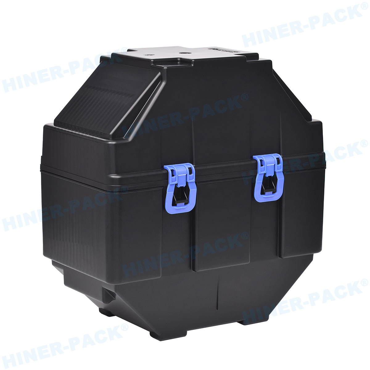
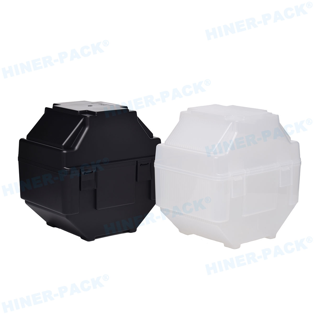
Front Opening Shipping Boxes (FOSB)
While FOUPs are primarily used for in-fab transport, FOSBs are designed for long-distance transport between wafer manufacturers and device fabs. FOSBs feature robust mechanical door-locking systems and internal cushioning mechanisms to secure the wafers during road and air transport. The structural configurations optimized by Hiner-pack ensure minimal contact wear on the wafer edges during transit.
Horizontal Wafer Shippers and Coin Category Carriers
For smaller wafer diameters (such as 100mm, 150mm, and 200mm) used in power semiconductors, MEMS, and optoelectronics, coin-style shippers are widely used. Wafers are stacked horizontally, separated by non-marring interleaf liners, and secured by a spring cushion lid. This structure prevents both lateral and vertical movement during global shipping.
Optimizing Mechanical Design for Yield Protection
The engineering details of a wafer container determine its protective efficiency. A well-designed wafer container for sale incorporates several key mechanical features:
Precision Slot Geometry: The internal combs or teeth that hold individual wafers must have precise spacing (pitch) and slope angles to ensure that wafers do not touch during vibration and are easily accessed by robotic end-effectors.
Spring Cushions and Retainers: For shipping configurations, flexible elastomer or polymer springs apply gentle pressure to the wafer edges, holding them securely in place without causing physical stress or micro-cracking.
Sealing Gaskets: High-purity thermoplastic elastomer (TPE) or fluoroelastomer gaskets are integrated along the door frame to provide an airtight seal, maintaining the interior micro-environment against outside air penetration.
AMHS Kinematic Coupling: The base of the carrier must feature high-tolerance kinematic coupling pins compliant with SEMI standards. This ensures precise positioning when docked on automated process tools.
Selecting the correct carrier configuration helps minimize yield loss caused by mechanical shocks and vibration during global logistics.
Industry Standardization and SEMI Compliance
Interoperability is crucial in the semiconductor manufacturing chain. Carriers must adhere strictly to SEMI (Semiconductor Equipment and Materials International) standards to operate correctly with load ports, atmospheric transfer modules, and robotic grippers from various equipment manufacturers.
Key standards include:
SEMI E47.1: Mechanical specifications for 300mm Front Opening Unified Pods (FOUP) used for wafer transport and processing.
SEMI E62: Specifications for kinematic coupling structures that define the physical docking interface of wafer carriers.
SEMI M31: Guidelines for securing and transporting silicon wafers to prevent structural damage and particulate deposition.
Compliance with these parameters ensures that when looking for a wafer container for sale, the chosen product will integrate smoothly into existing manufacturing lines without requiring expensive equipment modifications.
Sourcing Process and Operational Logistics
When procurement managers evaluate storage and transport carriers, several operational factors should be considered alongside material specifications:
Compatibility with Cleaning Cycles: Carriers undergo periodic cleanroom washing processes using deionized water, surfactant agents, and thermal drying. The materials must resist degradation, swelling, or loss of anti-static properties over repeated cleaning cycles.
Traceability Integration: Modern fabs rely on real-time tracking. Containers should feature dedicated areas for RFID tags or barcode placement, ensuring automated scanning systems can log carrier locations at every processing step.
Supplier Quality Control: Consistent manufacturing quality is essential. Every batch of carrier components must be tested for dimensional accuracy, surface resistivity, and particle outgassing properties before deployment in class 1 cleanroom environments.
For specific manufacturing configurations, Hiner-pack offers tailor-made options designed to meet the cleaning and compatibility requirements of modern fabrication processes.
Request Engineering Support and Product Details
Selecting appropriate wafer transport and packaging solutions is crucial for protecting semiconductor yields and ensuring seamless fab automation. To receive detailed specifications, engineering drawings, or product samples for your qualification processes, please submit your specific requirements to our technical sales team. We provide tailored configurations designed to match your processing parameters and cleanroom standards.
Contact our support representatives today to discuss your wafer dimensions, material requirements, and volume needs, and receive a formal quotation.
Frequently Asked Questions
Q1: What is the main difference between ESD-safe polymers and standard plastics used in wafer shipping?
A1: Standard plastics can accumulate static charges from friction, which attract airborne particulates and pose a risk of electrostatic discharge. ESD-safe polymers are embedded with conductive additives, such as carbon fiber or carbon powder, to achieve a surface resistivity of $10^5$ to $10^{11}$ ohms/sq. This allows static charges to dissipate safely without damaging active wafer circuitry.
Q2: Why is nitrogen purging necessary for wafer containers?
A2: Nitrogen purging replaces oxygen and moisture inside the container with clean, dry nitrogen gas. This prevents surface oxidation on copper or aluminum contact pads and prevents moisture from reacting with exposed silicon surfaces during transit and intermediate storage.
Q3: What dimensions are available when looking for a wafer container for sale?
A3: These containers are manufactured in standard sizes matching wafer diameters, primarily 100mm (4-inch), 150mm (6-inch), 200mm (8-inch), and 300mm (12-inch). Custom dimensions can also be manufactured for specialized substrates like gallium nitride (GaN) or silicon carbide (SiC).
Q4: How do mechanical cushions inside a shipping box protect wafer edges?
A4: Mechanical cushions apply localized, controlled spring force to the wafer edge, holding each substrate securely in its designated slot. This dampens shock and vibration during road and air transit, preventing wafers from shifting, rotating, or contacting the inner walls of the container.
Q5: How many times can a cleanroom wafer carrier be reused?
A5: The lifespan of a carrier depends on its material, structural wear, and washing frequency. High-purity PEEK or reinforced polycarbonate carriers can withstand hundreds of thermal and chemical cleaning cycles before material fatigue or dimensional variations require replacement.


