In semiconductor manufacturing, especially advanced packaging (fan-out,
2.5D/3D integration), wafer handling between processes demands containers that
go beyond simple storage. The market offers many wafer
containers for sale, but only a fraction meet the rigorous
particle, outgassing, and ESD specifications required for 200mm and 300mm
substrates. This guide provides a deep technical framework for procurement
engineers and fab managers, grounded in material properties, real contamination
mechanisms, and automation compatibility. We avoid generic advice and focus on
actionable parameters that affect die yield.
1. Industry Pain Points: Why Standard Carriers Fail in High-Volume
Packaging
High-density packaging lines subject wafers to repeated vacuum cycles,
thermal excursions (up to 260°C for solder reflow), and mechanical vibrations
from overhead hoist transport (OHT). Standard polypropylene or polycarbonate
containers often induce three failure modes:
Particulate shedding – Molded edges or static charge
accumulation attracts sub-0.1µm particles, causing killer defects in hybrid
bonding.
Ionic/volatile contamination – Unoptimized polymer
additives release amines or plasticizers that fog cu low-k dielectrics.
Warpage-induced micro-cracks – Non-uniform support points
amplify stress on 50µm thin wafers during lateral transport.
Over 34% of packaging rework incidents trace back to wafer container-related
damage (internal industry audits, 2024–2026). Therefore, evaluating wafer
containers for sale requires verifying not only dimensional
tolerances but also certified cleanliness according to SEMI E49.5 and ESD STM
12.1.
2. Core Technical Parameters for Wafer Containers in Advanced Packaging
When sourcing wafer containers, the following five engineering metrics serve
as non-negotiable filters. Each directly impacts post-packaging assembly
yield.
2.1 Material Composition & Outgassing Control
High-purity polyetheretherketone (PEEK) or perfluoroalkoxy (PFA) containers
dominate for 300mm FOUPs/FOSBs due to low moisture absorption and outgassing
below 0.1 µg/cm². For cost-sensitive 200mm lines, static-dissipative
polycarbonate (PC) with carbon nanotube (CNT) loading is acceptable if volatile
organic compound (VOC) emission is verified via GC-MS to be <50 ng/g (ISO
14644-14). Avoid metals or coated surfaces that flake.
2.2 Particle Retention & Surface Roughness
Inner surface average roughness (Ra) ≤ 0.4 µm prevents particle
entrapment.
Dynamic particle generation test (ISO 14644-15): Class 1 at rest, Class 2
during simulated vibration (10 Hz–500 Hz).
Gate vestiges or ejector pin marks must be located outside wafer peripheral
exclusion zone (≥ 10mm from wafer edge).
2.3 ESD Protection & Surface Resistivity
Advanced packaging uses sensitive GaAs or InP wafers (ESD sensitivity <
200V). Containers require surface resistivity between 1E5 and 1E12 ohms/sq
(dissipative range). Full conductive materials (1E3–1E5) risk electrochemical
migration. Wafer containers for
sale that lack ESD certification per ANSI/ESD S20.20 should be
excluded.
2.4 Dimensional Stability & Die-Stack Clearance
With wafer thinning down to 50µm, support ribs must distribute contact
pressure evenly. Calculate contact area using finite element analysis (FEA) to
avoid peak stress > 5MPa. For multiple-wafer stacks, inter-wafer spacers must
maintain minimum 2mm gap to accommodate micro-bumps or TSV protrusions.
2.5 Automation Interface
All containers must conform to SEMI E57 (mechanical interface for 300mm) or
E15 (for 200mm). Key dimensions: pitch accuracy ±0.2mm, latch engagement force
4–6N, and RF-ID pocket depth 12.5mm for tool tracking. Non-compatible units
disrupt factory scheduling.
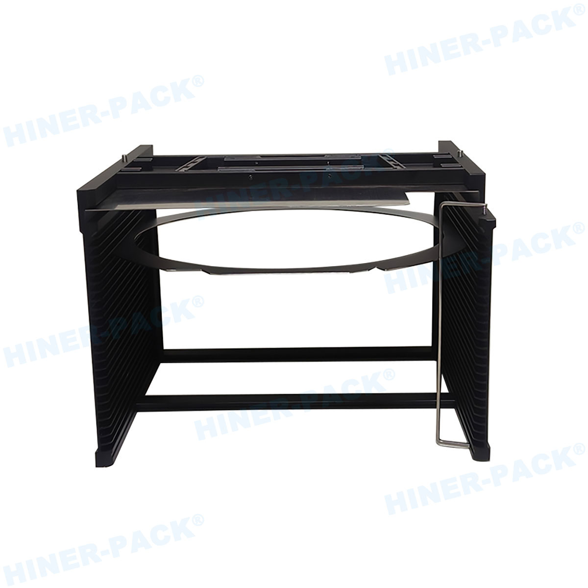
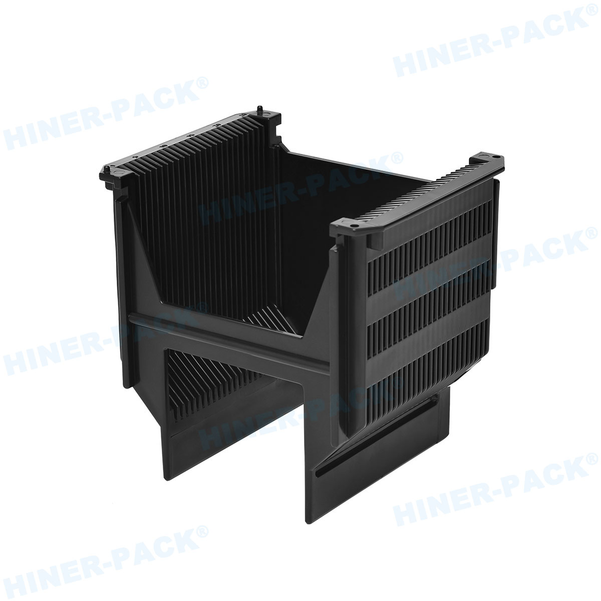
3. Configurations Based on Packaging Process Stage
Different wafer containers serve distinct roles: from incoming inspection to
die attach. Selecting the wrong type multiplies handling defects.
3.1 Single-Wafer Shipper (SWS) for Thin or Warped Substrates
SWS designs incorporate cushioned inner rings and vacuum-sealed inner pods.
They are mandatory for wafers after backgrinding (< 150µm) or those with
large bow (> 500µm). The elastic ring conforms to wafer curvature,
maintaining edge exclusion. Typical order volume: 200–500 units for pilot
packaging lines. Many wafer containers for
sale in this category fail bow accommodation – verify with
bow-up/bow-down tests per SEMI G86.
3.2 Multi-Wafer Carriers for Batch Diffusion or Plating
Horizontal carriers (stacked slots) suit wet processes like electroplating;
vertical carriers (parallel slots) reduce cross-contamination in PVD. Slot pitch
uniformity must be within ±0.05mm to avoid wafer edge chipping. For 12-inch
multi-wafer cassettes, maximum load ≤ 25 wafers with reinforced side struts to
prevent bowing during heat curing (150°C for 2 hours).
3.3 FOUP-Compatible Shipping Boxes for Inter-Fab Transfer
These are outer boxes that host FOUPs or FOSBs, adding foam shock absorption
and moisture barrier. Requirements: seal integrity after 100 drops (ISTA 3A),
internal humidity ≤ 40% after 48h. Inner latch passivation to prevent aluminum
fluoride buildup.
4. Validating Supplier Claims: Cleanliness & Particle Protocols
Many wafer container suppliers provide generic ISO 5 cleanroom photos but
lack lot-level test data. Implement a three-step validation before bulk
purchase:
Step 1 – Liquid particle count (LPC): Extract with
ultrapure water (UPW) and count particles ≥ 0.1µm per cm² (limit: <
100/cm²).
Step 2 – Airborne molecular contamination (AMC): Use wafer
surface analysis via thermal desorption GC-MS; sulfuric acid limits < 0.05
µg/wafer equivalent.
Step 3 – Dynamic mechanical testing: Mount container on
vibration table (3Grms, 20–2000Hz) for 30 min, then measure particles on witness
wafer (defects < 0.1/cm²).
Reputable sources offering wafer containers for
sale will provide these test reports without non-disclosure delays.
Hiner-pack maintains on-site
particle lab per ISO 17025, ensuring every batch meets customized spec limits –
a differentiator from generic stock containers.
5. Material Selection Deep Dive: PC vs. PFA vs. Conductive PEI
Selecting material influences both yield and long-term storage cost
(excluding TCO). But focus on technical compatibility:
Polycarbonate (PC): Suitable for 200mm wafer handling in
backend assembly (temp < 125°C). Antistatic grades exist but lose resistivity
after 50 autoclave cycles. Avoid using with aggressive solvents (acetone, IPA
> 30%).
Perfluoroalkoxy (PFA): Superior chemical resistance (HF,
H2SO4) and thermal stability up to 260°C. Ideal for wet etch or solvent cleaning
steps. Higher weight (density 2.15 g/cm³) may require robot re-calibration.
Conductive polyetherimide (PEI): Combines low outgassing
(NASA low outgas certified), inherent flame resistance (UL 94 V-0), and surface
resistivity 1E6 – 1E9 ohms/sq. Preferred for 300mm vacuum processing. Molding
complexity raises lead time to 6 weeks.
Hiner-pack engineers provide
compatibility matrices cross-referencing your fab’s chemical use, temperature
profile, and ESD requirements – reducing selection errors common in
off-the-shelf purchases.
6. Packaging & Logistics Considerations for Wafer Containers
Even well-designed containers suffer contamination during transit if not
double-bagged in ESD-safe, static-dissipative nylon bags with desiccant packs.
For international shipments, ensure:
Outer cartons pass ISTA 2A drop test (76cm height).
Barrier bag oxygen transmission rate < 0.5 cc/100in²/day.
Vacuum-sealed inner bag with humidity indicator card (target < 20%
RH).
When you evaluate wafer containers for
sale, ask for a packaging validation report specific to your
logistics route (air vs. sea freight). Some vendors skip this, leading to
moisture absorption that causes haze on wafer surfaces.
7. Frequently Asked Questions (Engineering Focus)
Q1: Can the same wafer container be used for both 200mm and 150mm
wafers with adapters?
A1: Not recommended for automated lines. Adapters often
create asymmetric force distribution, increasing edge particle generation. For
manual R&D handling, some PFA containers with stepped inserts exist, but
they must be re-qualified for vibration and ESD. We advise separate dedicated
carriers for each wafer diameter.
Q2: How to validate the static decay time of a wafer container
without expensive meters?
A2: Use a verified surface resistance megohmmeter per
ANSI/ESD SP15.1. However, decay time testing requires a charge plate monitor
(CPM). Simple proxy: measure surface resistivity from point to point (< 1E12
ohms) – if > 1E12, static decay will exceed 2 seconds, risking ESD. Most
qualified suppliers provide decay time data (typically < 0.5 sec).
Q3: Are reusable wafer containers allowed for high-volume packaging
with mixed product types?
A3: Yes, but only if robust cleaning protocols (e.g.,
deionized water jet + hot air drying) are validated between batches. Organic
residues from one device type can cross-contaminate subsequent wafers. Suppliers
like Hiner-pack offer cleaning
validation kits to test for residual ionic contamination after 50 reuse cycles.
Single-use containers are preferred for sensitive GaAs devices.
Q4: What SEMI standards must a container comply with for 300mm FOUP
applications?
A4: Minimum SEMI E47 (specification for 300mm FOUP), E57
(kinematic coupling), E62 (load port mapping), and E154 (mechanical and
electrical interfaces). Also reference SEMI E176 for AMC control. Any wafer
containers for sale lacking these certificates cannot interface
with standard EFEMs.
Q5: How to mitigate damage from wafer vibration during overland
transport?
A5: Use containers with integrated shock-absorbing foam
(polyurethane density 35 kg/m³) and lock the wafer retainer clip. Place the
container inside an outer corrugated box with edge protectors. Perform ISTA 3E
simulation for less-than-truckload (LTL) shipping. Field data show that adding
gel-based vibration dampers reduces micro-crack incidence by 62%.
Q6: Can containers be autoclaved for sterile packaging applications
(e.g., medical MEMS)?
A6: Only PFA or PEEK containers withstand repeated autoclave
(121°C, 15 psi) without degradation. PC containers will stress-crack after 2
cycles. Look for "autoclavable" marking and verify material data sheet for
hydrolytic stability. Hiner-pack provides PFA
containers with 500-cycle autoclave validation.
Selecting the right wafer carrier requires matching
material science, cleanliness certification, and automation compatibility. For
engineering data sheets, sample qualification kits, or batch quotes, contact our
team directly. Inquire now about certified wafer
containers for sale with full SEMI/GMP documentation.


