
In semiconductor manufacturing, transporting silicon wafers between fabrication facilities, packaging plants, and end-testing sites requires specialized protective packaging. Every stage of transport exposes fragile silicon structures to physical vibration, electrostatic discharge (ESD), and airborne molecular contamination (AMC). While procurement departments must manage operational overhead, evaluating a wafer box price requires an understanding of material science, manufacturing tolerances, and cleanliness standards. Balancing initial packaging costs against wafer yield protection is a primary challenge for modern semiconductor supply chain managers.
As microchip geometries shrink to single-digit nanometer levels, the tolerance for physical and chemical contamination decreases. Packaging solutions from manufacturers like Hiner-pack are engineered to protect these high-value components. Understanding how different engineering choices affect the wafer box price helps organizations make informed sourcing decisions that prevent costly wafer degradation during transit.
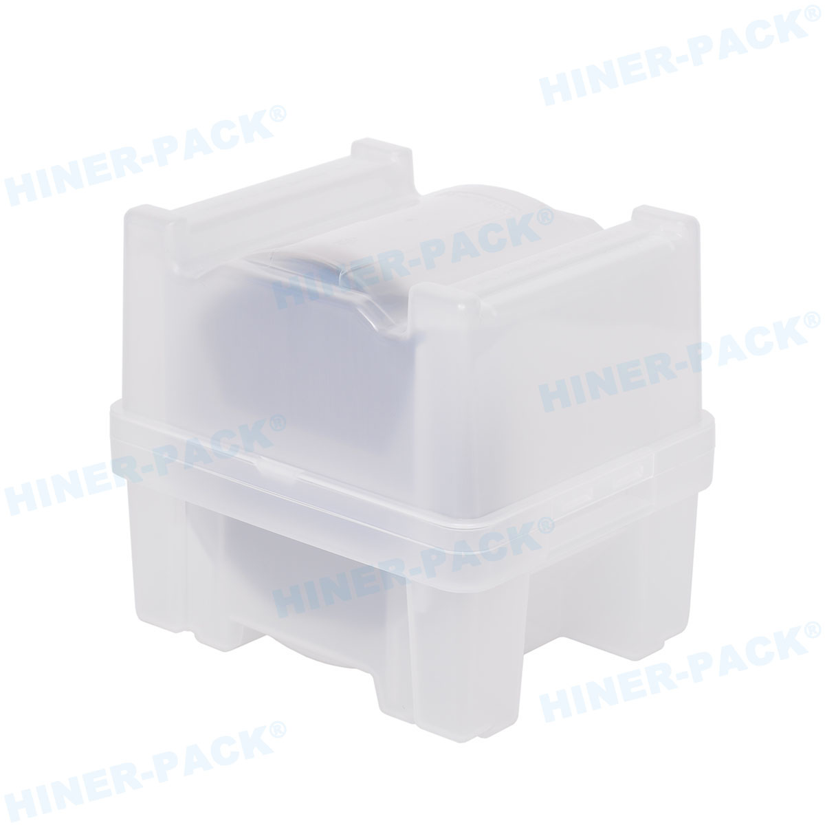
Material Science: The Primary Driver of Wafer Box Price
The choice of polymer substrate is the most significant factor determining the overall wafer box price. Standard shipping containers and process cassettes are fabricated from high-purity plastics, each selected for specific mechanical and chemical properties.
Polypropylene (PP) vs. Polycarbonate (PC)
Polypropylene is widely used for cost-effective, short-range transport of non-critical wafers or raw silicon substrates. PP offers reasonable impact resistance and chemical compatibility, keeping the entry-level wafer box price relatively low. However, PP has higher outgassing rates and lower structural rigidity compared to engineering polymers. For advanced nodes, polycarbonate is preferred. PC provides superior dimensional stability, lower outgassing profiles, and high impact resistance, though it commands a premium in the market.
Specialized Conductive and Antistatic Additives
Raw polymers are naturally insulating, meaning they can accumulate electrostatic charge through friction during transport—a phenomenon known as tribocharging. To prevent ESD-induced damage to integrated circuits, wafer boxes must possess static-dissipative or conductive properties. Incorporating carbon powder, carbon fibers, or specialized inherently dissipative polymers (IDPs) into the plastic matrix increases manufacturing complexity. This material modification directly increases the wafer box price, but it is necessary for safeguarding patterned wafers.
High-Performance Fluoropolymers
For high-temperature processing or extreme chemical cleanliness, materials like PFA (Perfluoroalkoxy) or PEEK (Polyetheretherketone) are utilized. These materials offer minimal outgassing, high chemical inertness, and exceptional thermal stability. Because the raw material costs of fluoropolymers are significantly higher and require specialized molding equipment, containers utilizing these polymers sit at the highest tier of the pricing spectrum.
Form Factors and Automation Interfaces
Wafer dimensions and automation requirements dictate the physical design of the packaging, which heavily influences the tooling, molding, and testing expenses associated with production.
Standardized sizes—such as 100mm (4-inch), 150mm (6-inch), 200mm (8-inch), and 300mm (12-inch)—require different structural support. Larger wafers possess greater mass and flexibility, demanding more robust enclosure designs to prevent warping or mechanical contact during transit. A 300mm Front Opening Shipping Box (FOSB) is highly complex, featuring robotic handling flanges, precise latching mechanisms, and gas purge capability, which makes its wafer box price substantially higher than a simple 200mm horizontal wafer shipper.
The integration of automated material handling systems (AMHS) in modern fabs requires strict adherence to SEMI (Semiconductor Equipment and Materials International) standards. Every alignment notch, door latch, and pocket tolerance must be manufactured with sub-millimeter precision. Producing molds that achieve these exact tolerances requires advanced machinery and regular calibration, contributing directly to the amortized wafer box price for SEMI-compliant designs.
Cleanroom Manufacturing and Quality Control Standards
The environment in which a wafer box is manufactured, cleaned, and packaged is just as important as the material itself. A high-quality container must be free of particulate contamination before it ever enters a fabrication facility.
Industrial packaging suppliers like Hiner-pack operate certified cleanrooms (ranging from ISO Class 4 to ISO Class 6) to perform injection molding, assembly, and final packaging of shipping containers. Operating these facilities requires continuous air filtration, strict garment protocols, and regular testing for airborne particulates. The overhead costs of maintaining these environments are reflected in the wafer box price, but this cleanroom processing is what prevents micro-particulate contamination from landing on wafer surfaces and causing device failures.
Beyond cleanroom assembly, premium shipping containers undergo extensive cleaning processes, including multi-stage deionized water baths and ultrasonic cleaning to remove surface ionic contaminants and residues. Analytical testing, such as Liquid Chromatography-Mass Spectrometry (LC-MS) to detect trace organic outgassing, is performed on batch samples. These quality assurance steps add production time and require sophisticated laboratory equipment, further differentiating high-end wafer boxes from generic plastic alternatives.
Evaluating the Total Cost of Ownership (TCO)
Procurement teams often focus solely on the initial wafer box price, yet a more accurate metric is the total cost of ownership over the product lifecycle. A low-cost shipper that suffers from rapid material degradation or causes wafer damage represents a high liability.
Reusability and Durability: Premium wafer boxes constructed from high-grade polycarbonate or carbon-filled materials can withstand multiple washing and shipping cycles without losing structural integrity or ESD properties. Over several transit cycles, a durable box proves more cost-effective than a single-use container.
Yield Protection: The financial loss associated with a single scratched, contaminated, or electrostatic-damaged wafer cassette can easily exceed the cost of an entire shipment of premium wafer boxes. Investing in superior structural packaging is a form of risk mitigation for high-value wafer lots.
Process Compatibility: Standardized, high-precision boxes reduce downtime caused by robotic handling errors in automated fabs. Secure latching and precise pocket dimensions minimize wafer rattling, protecting delicate microscopic structures during international air freight.
Procurement Strategies to Balance Costs
Acquiring wafer transport solutions requires strategic planning to balance budget allocations with production standards. Working directly with specialized manufacturers allows semiconductor packaging engineers to identify the correct specifications without over-specifying requirements.
Purchasing wafer shippers in high volumes is a practical method to lower the per-unit wafer box price. Since injection molding setup costs are substantial, long production runs allow manufacturers to distribute these fixed costs over larger quantities. Consolidating annual demand and establishing long-term supply agreements with partners like Hiner-pack ensures stable pricing and consistent material availability, which is particularly beneficial during periods of global resin supply fluctuations.
Collaborating with the supplier’s engineering team during the selection process can also yield cost efficiencies. If wafers are only being transported short distances between cleanrooms on the same campus, a simpler, non-hermetic shipping cassette may suffice, avoiding the higher expenses associated with vacuum-sealed, gas-purged FOSBs. Matching the packaging specification precisely to the transport environment is key to avoiding unnecessary expenditures.
Inquiry and Custom Consultation
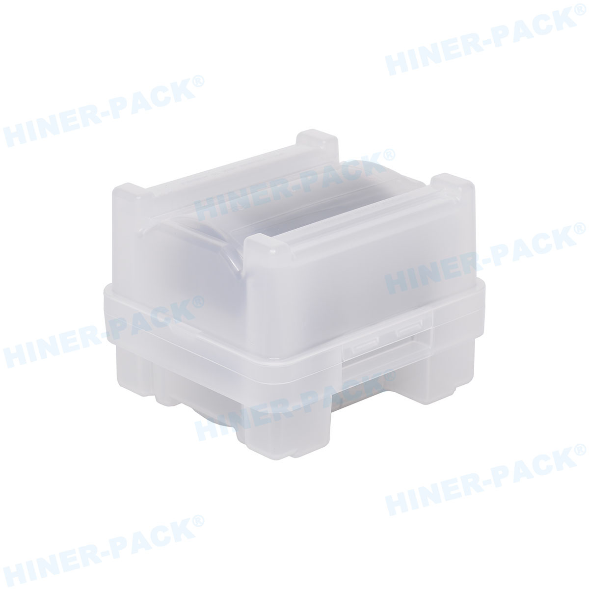
Selecting the appropriate wafer transport container requires balancing material characteristics, cleanliness requirements, and budget constraints. Hiner-pack provides a comprehensive range of wafer shipping boxes, coin shippers, and storage cassettes manufactured to meet rigorous industry standards. To receive a detailed quotation tailored to your specific wafer sizes, ESD requirements, and volume needs, please contact our sales and engineering team for an official inquiry. We are prepared to assist you in finding a balance between wafer box price and yield protection.
Frequently Asked Questions
Q1: Why is there such a significant difference in wafer box price between 200mm and 300mm shipping containers?
A1: The price difference is driven by design complexity and automation requirements. While 200mm wafers are often transported in simpler horizontal shippers or standard cassettes, 300mm wafers require Front Opening Shipping Boxes (FOSBs) or FOUPs. These 300mm containers must feature highly precise robotic interfaces, complex door latching mechanisms, vacuum-gasket seals, and gas purge capabilities to comply with SEMI standards. The material volume, tooling complexity, and quality testing for 300mm automated transport are substantially higher, leading to a higher unit cost.
Q2: How do ESD additives affect the long-term usability and cost of a wafer box?
A2: ESD protection is achieved by compounding polymers with conductive carbon additives or inherently dissipative polymers (IDPs). These additives increase the material raw cost and require careful processing during injection molding to ensure uniform distribution of electrical properties. Over time, lower-grade carbon additives can shed carbon particles, which presents a contamination concern. Higher-quality wafer boxes use advanced, non-sloughing dissipative compounds that maintain their static protection through multiple cleaning cycles, justifying their higher initial wafer box price by offering a longer operational lifespan.
Q3: Can wafer boxes be reconditioned and reused to offset a higher initial purchase price?
A3: Yes, high-quality wafer boxes made from durable polycarbonate or PEEK are designed for multiple reuse cycles. However, reuse requires a strict reconditioning protocol, including ultrasonic cleaning in deionized water, vacuum drying, and particle inspection in a certified cleanroom environment. If a box shows signs of physical wear, latch degradation, or loss of ESD properties, it must be retired. Implementing a structured reuse program with a qualified packaging manufacturer like Hiner-pack can significantly lower the per-shipment packaging cost over time.
Q4: How does outgassing potential impact the pricing of wafer shipping containers?
A4: Outgassing refers to the release of volatile organic compounds (VOCs) from plastic materials, which can condense onto wafer surfaces and cause chemical contamination. Low-outgassing polymers, such as high-purity polycarbonate blends or fluoropolymers, undergo specialized manufacturing and purification processes to remove residual monomers and solvents. The extensive testing, raw material certification, and advanced processing required to guarantee extremely low outgassing levels are key factors that elevate the wafer box price for advanced semiconductor applications.
Q5: Does cleanroom packaging at the manufacturer's site add to the final wafer box price?
A5: Yes, cleanroom packaging adds a minor premium to the cost, but it is necessary for maintaining wafer yield. If a wafer box is manufactured and packed in a standard industrial environment, it will carry atmospheric dust and plastic particles. When introduced into a semiconductor fab, these particles transfer directly to the silicon wafers, causing lithography defects. Shipping containers processed in ISO Class 4 or 5 cleanrooms and double-bagged in ultra-clean polyethylene film arrive ready for immediate introduction into the fab cleanroom, saving the customer from expensive on-site pre-cleaning steps.














