
Compound semiconductor manufacturing, silicon wafer processing, and precision optoelectronic fabrication require protective logistics pipelines. Standard packaging solutions fail to meet the cleanroom cleanliness levels and electrostatic discharge protection required for raw substrates. The containers used to transport these sensitive components must prevent physical damage, electrostatic buildup, and microscopic chemical contamination.
Acquiring a reliable wafer canister quotation requires a deep understanding of both material science and cleanroom manufacturing standards. Procurement managers and packaging engineers must look beyond the initial unit price to evaluate how raw material selection, physical design, and post-injection processing impact the total cost of ownership. This analysis explores the technical parameters, manufacturing methodologies, and procurement strategies that govern wafer container pricing.
Material Integrity and Electrostatic Properties
The structural foundation of a semiconductor shipping canister is its base polymer. The choice of raw material directly impacts the price structure presented in any wafer canister quotation, as engineering-grade resins carry varying cost profiles depending on their physical and electrical properties.
Surface Resistivity and ESD Protection
Unmodified polymers generate high electrostatic charges through friction during transit. To prevent electrostatic discharge damage to integrated circuits or sensitive epitaxial layers, canisters are fabricated using specialized compounds:
Conductive Materials: Typically carbon-filled polymers with a surface resistivity of 103 to 105 ohms/square. These materials provide rapid charge dissipation but require careful grounding strategies.
Static Dissipative Materials: Materials with a surface resistivity of 106 to 1011 ohms/square, offering a controlled rate of charge decay. These are preferred for sensitive device handling.
Natural/Antistatic Polymers: Virgin polypropylene or polystyrene with temporary or permanent antistatic additives. While more economical, their long-term static protection varies based on humidity and age.
Outgassing and Chemical Stability
During storage and shipping, volatile organic compounds (VOCs) can outgas from the plastic body, depositing a thin molecular film on the wafer surface. This film interferes with subsequent deposition and etching steps. High-purity polypropylene (PP) and specialty polycarbonate (PC) resins are selected for low-outgassing properties. Resins certified for minimal trace metal content and low ionic contamination command a premium in the market, directly influencing the baseline material costs in a quotation.
Physical Engineering and Structural Tolerances
Beyond the material science, the mechanical architecture of the container determines its protective capabilities during global transit. Mold precision and structural wall thickness are key cost drivers in high-precision manufacturing.
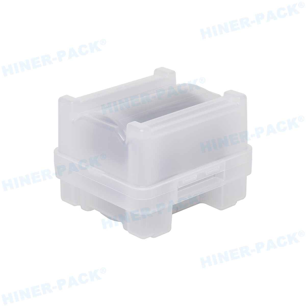
Mechanical Architecture of Coin-Style Shippers
Coin-style wafer shippers, or individual canisters, are engineered to hold single or multiple wafers securely without shifting. The internal cavity must feature exact dimensional tolerances. If the cavity is too wide, the wafer will slide horizontally, causing edge chipping. If the cavity is too narrow, thermal expansion can compress the wafer, leading to physical fractures.
To mitigate these movements, manufacturers integrate specialized wafer retention components:
Silicone-Free Elastomeric Cushions: Placed at the bottom or top of the canister to absorb vertical vibrations.
Internal Spring Systems: Molded plastic springs that exert a gentle, continuous downward force to keep the wafer planar.
Precision Latches: Secure locking mechanisms that prevent accidental opening during automated handling or manual sorting.
Wall Thickness and Drop Resistance
To survive the physical impacts of industrial shipping, the canister walls must resist deformation. Thicker-walled canisters provide superior impact absorption but require more raw material and longer cycle times during the injection molding process. High-performance designs feature external ribbing to increase rigidity without adding unnecessary weight, balancing material cost with physical protection.
Cleanroom Processing and Contamination Control
A significant portion of a wafer canister quotation is determined by the environmental conditions of the manufacturing facility. Injection-molded plastics are naturally susceptible to attracting airborne particles due to triboelectric charging during the cooling phase.
Class 100 (ISO 5) Packaging Environments
For semiconductor-grade shipping containers, standard industrial manufacturing is insufficient. The canisters must be molded, cleaned, inspected, and packaged within certified cleanroom environments. This process involves several distinct operational phases:
Deionized Water Rinsing: Canisters undergo multi-stage washing with high-purity deionized water to remove surface particles and ionic residues.
Ultra-Pure Nitrogen Drying: Surfaces are dried using filtered nitrogen to prevent water spotting and chemical deposition.
Double-Bag Packaging: The clean canisters are sealed inside dual-layer, ultra-clean polyethylene bags within a Class 100 environment, ensuring the interior remains uncontaminated until opened in the customer's fab.
The operational overhead of maintaining these cleanroom environments, alongside regular particle testing and certified liquid particle counts (LPC), represents a core component of the manufacturing service fee included in the price structure.
Commercial Dynamics of the Wafer Canister Quotation
When procurement departments analyze a wafer canister quotation, they must evaluate several commercial variables that influence the final unit cost. Understanding these dynamics allows for more realistic budgeting and supply chain planning.
Volume Scaling and Injection Tooling
Injection molding is a highly volume-dependent process. The initial setup, including mold installation, material purging, and cleanroom calibration, represents a fixed cost. Consequently, larger order volumes distribute these setup costs over a greater number of units, significantly lowering the individual unit price. Standard multi-cavity molds produce several canisters per cycle, reducing manufacturing time and labor overhead for high-volume contracts.
Customization and Substrate Sizes
While standard wafer sizes (such as 100mm, 150mm, 200mm, and 300mm) benefit from standardized, high-volume tooling, non-standard substrates require specialized packaging. Wafers made from Gallium Arsenide (GaAs), Silicon Carbide (SiC), or thin glass often require custom internal heights, modified spring tensions, or unique ESD profiles. Developing custom molds involves capital expenditure for tooling, which must be factored into the initial quotation either as an upfront charge or amortized over a specific purchase agreement.
Hiner-pack addresses these variable requirements by offering both standardized cleanroom-compatible shippers and tailored packaging engineering services. This ensures that the physical dimensions of the canister match the specific thickness and fragility of the target substrate.
Addressing Semiconductor Logistics Challenges
Evaluating packaging materials based solely on procurement cost can lead to systemic failures in the logistics chain. Investing in high-grade transport canisters prevents several common semiconductor industry issues.
Preventing Mechanical Edge Chipping
During air transit, packages experience continuous high-frequency vibrations. If the internal tolerances of the canister allow for micro-movements, the wafer edges can rub against the container wall, generating micro-particles and causing structural micro-cracks. High-precision canisters hold the wafer securely at its perimeter, preventing lateral movement and preserving the integrity of the active die area.
Eliminating Surface ESD Damage
Electrostatic discharge can destroy sub-micron features on patterned wafers without leaving visible physical marks. By utilizing static dissipative polymers with consistent surface resistivity, the static charges generated during handling are safely bled away rather than discharging through the sensitive circuit structures.
Minimizing Haze and Surface Contamination
Chemical contamination on a wafer can ruin an entire lithography batch. Using low-outgassing, additive-free raw materials ensures that no organic compounds migrate from the packaging to the wafer surface, preserving the yield rate of high-value epitaxy processes.
Evaluating Your Packaging Procurement Strategy
Before finalizing a purchase agreement, procurement professionals should establish a standardized framework for evaluating alternative packaging options. The following checklist outlines the essential parameters that should be clarified before requesting a quotation:
Identify the exact wafer diameter, thickness, and fragile edge zones.
Specify the required ESD classification (conductive, static dissipative, or antistatic).
Define the acceptable particulate limits and cleanroom packaging standard (e.g., ISO Class 5 double-bagged).
Determine the projected annual volume and release schedule to optimize production runs.
Verify the compatibility of the canister design with existing automated sorting and pick-and-place equipment.
To receive a customized wafer canister quotation from Hiner-pack, please prepare your specific material requirements, wafer dimensions, and expected volume metrics. Our technical sales team provides detailed specifications and material certifications to ensure complete compatibility with your cleanroom protocols and logistics requirements.
Frequently Asked Questions
Q1: What materials are standard for ESD-safe wafer canisters?
A1: Standard materials include carbon-filled conductive polypropylene (PP) or polycarbonate (PC) for low resistivity, as well as inherently dissipative polymers. The selection depends on the target surface resistivity, outgassing limits, and structural strength required for the specific shipping application.
Q2: How does cleanroom packaging affect the final wafer canister quotation?
A2: Cleanroom manufacturing, deionized water washing, and double-bagging under ISO Class 5 or Class 6 conditions add to the processing cost. However, this step is necessary to ensure the canisters do not introduce foreign particulate contamination to the cleanroom environments of semiconductor fabrication facilities.
Q3: Can wafer canisters be washed and reused?
A3: Yes, many high-purity canisters made from durable polymers like polycarbonate can be re-cleaned using specialized automated washing systems. However, the integrity of the antistatic properties must be monitored, as repeated washing cycles can deplete temporary topical antistatic additives in lower-grade materials.
Q4: Why are custom sizes more expensive than standard 200mm or 300mm canisters?
A4: Standard sizes benefit from high-volume, multi-cavity production lines and amortized tooling costs. Custom sizes for unique wafer thicknesses or non-standard diameters require dedicated mold fabrication, smaller production runs, and custom machine calibration, which increases the unit cost.
Q5: How do outgassing properties affect wafer yield during transport?
A5: Low-grade plastics can release volatile organic compounds over time. When sealed inside shipping bags, these VOCs settle onto the wafer surface as chemical contamination, leading to adhesion failures or defects during subsequent deposition and lithography processes. Using certified low-outgassing materials prevents this issue.














