
Safe transport of silicon wafers during semiconductor manufacturing demands highly specialized packaging solutions. Wafer canisters, designed to safeguard delicate silicon substrates from physical shock, particulate contamination, and electrostatic discharge (ESD), represent a significant procurement consideration for front-end and back-end cleanroom operations. When engineering and procurement departments evaluate these packaging components, understanding the underlying drivers of the wafer canister price is necessary for balancing mechanical protection with budget considerations.
The pricing of wafer shipping canisters is not a uniform metric. It is dictated by a complex combination of material purity, cleanroom production requirements, physical dimensional tolerances, and electrostatic mitigation capabilities. By evaluating these elements, packaging engineers can specify the exact container required for their specific wafer diameters and surface sensitivities without over-specifying and incurring unnecessary production expenses.
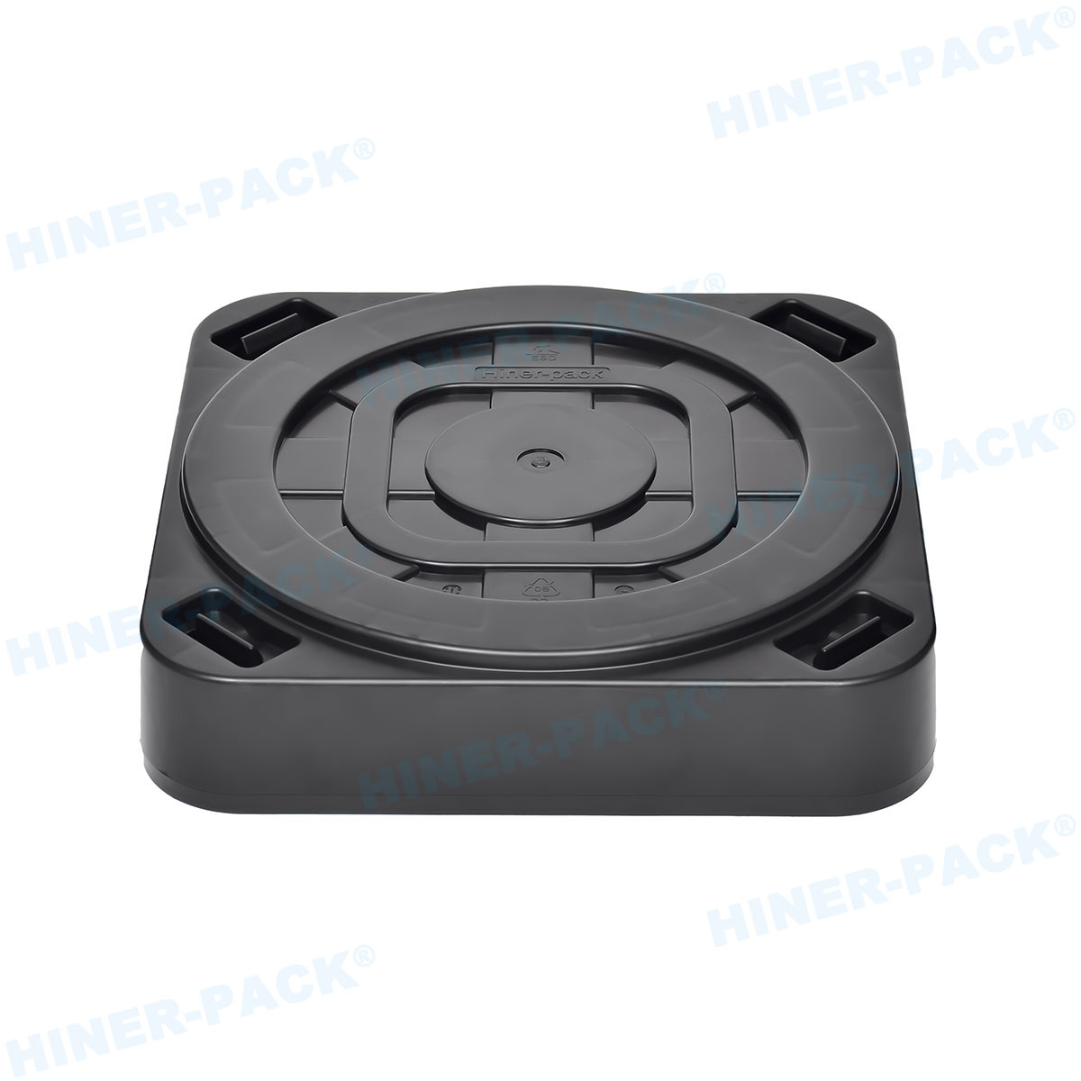
1. Polymer Formulation and Material Purity Drivers
The primary element dictating the market value of wafer transport containers is the raw material composition. Semiconductor wafers are highly sensitive to chemical outgassing and ionic contamination, which can degrade thin-film structures and alter electrical performance. Standard shipping containers use diverse polymer formulations depending on the cleanliness required for different process nodes.
Polycarbonate (PC) is widely utilized for its mechanical impact resistance, dimensional stability, and optical clarity. For high-purity shipping applications, carbon-fiber-filled polycarbonate or specialized conductive polymers are integrated to establish continuous ESD protection. The refinement process of these engineering plastics directly influences the wafer canister price. High-purity, low-outgassing resins command a premium compared to recycled or lower-grade structural plastics, as they undergo rigorous filtration to minimize trace metals and volatile organic compounds (VOCs).
In ultra-clean environments where thermal resistance and chemical inertness are paramount, advanced fluoropolymers like PFA (Perfluoroalkoxy) or high-performance PEEK (Polyetheretherketone) are selected. These materials provide outstanding thermal stability and chemical resistance during transport of highly sensitive substrates, yet their compound synthesis and processing requirements push the acquisition pricing higher. Choosing the appropriate material class ensures that the wafer container matches the thermal and chemical realities of the fab process floor.
2. Cleanroom Manufacturing and Contamination Control Standards
The manufacturing environment where wafer canisters are molded, assembled, and packaged plays a significant role in determining final market pricing. To prevent microscopic particulates from settling on the structural surfaces of the carriers, precision injection molding must occur within certified cleanroom environments.
Facilities operated by specialized manufacturers such as Hiner-pack utilize ISO Class 5 (Class 100) or ISO Class 6 (Class 1000) cleanrooms for manufacturing, inspection, and ultra-pure packaging. The operation of these controlled environments requires substantial utility support, HEPA filtration maintenance, and strict personnel protocols. This operational overhead is factored into the production output, directly correlating with the market pricing of the finished products.
In addition to cleanroom molding, post-mold processing heavily affects cleanroom compatibility. Canisters must undergo deionization processes, specialized aqueous cleaning cycles, and vacuum sealing in double-layer ESD-safe poly bags. These processing steps minimize particle counts and prevent tribocharging during transit. The level of testing required—such as liquid particle counting (LPC) and ion chromatography—adds steps to the quality control pipeline, reflected in the final unit pricing.
3. Dimensional Engineering and Structural Configuration
The structural design of the canister determines its mechanical integrity during global logistics. Shipping containers are engineered to hold wafers of specific diameters, typically ranging from 76mm (3 inches) to 300mm. The dimensional tolerances and structural complexity of these carriers scale with wafer size, directly influencing the mold complexity and manufacturing cycle times.
As wafer size increases, the mechanical strain on the carrier structure during transit becomes more pronounced. A 300mm canister requires robust wall thickness, reinforced structural ribbing, and sophisticated internal retention systems to prevent wafer movement. The design of inner cushions, silicone retaining springs, and high-purity elastomer gaskets is engineered to absorb shock and vibration. These physical additions to the container construction increase the bill of materials, which ultimately affects the overall wafer canister price.
Beyond standard multi-wafer jars, coin-style single wafer shippers are frequently used for shipping highly valuable individual die or thin wafers. These designs feature precision-engineered internal geometries that secure the wafer edge, preventing surface contact with the canister lid. The precision required to mold these non-contact edge-grip mechanisms involves tight tolerance controls, which influences manufacturing yield rates and unit pricing.
4. ESD Protection and Surface Resistivity Specifications
Electrostatic discharge is a primary cause of device failure during wafer transport and handling. To mitigate this hazard, wafer packaging must exhibit controlled electrical properties. Canisters are classified based on their surface resistivity into conductive, dissipative, or anti-static categories.
Conductive Materials (Surface Resistivity < 106 ohms/sq): These compounds contain carbon additives that provide rapid charge decay. They are often opaque and structurally rigid.
Static Dissipative Materials (Surface Resistivity 106 to 1011 ohms/sq): These provide a controlled discharge path, protecting sensitive gate oxides from electrostatic damage during manual or automated extraction.
Insulative Materials (Surface Resistivity > 1012 ohms/sq): Standard transparent plastics that require anti-static surface treatments, which may degrade over time or during wash cycles.
Developing polymers with permanent static dissipative properties that do not rely on migratory anti-static agents is a complex chemical process. Migratory agents can transfer to the wafer surface, leaving organic residues that interfere with subsequent lithography or deposition steps. Permanent ESD-safe materials require specialized compounding with carbon nanotubes or inherently dissipative polymers. This advanced chemical engineering is a primary driver behind variations in the wafer canister price, as cleaner, more reliable ESD protection requires more sophisticated raw materials.
5. Sourcing Volume, Customization, and Supply Chain Integration
Industrial B2B procurement is heavily dependent on volume commitments and supply chain logistics. Large-scale semiconductor fabs require consistent deliveries of packaging materials to maintain uninterrupted production lines. Buying in high-volume production runs allows manufacturers to amortize setup costs, cleanroom preparation, and tooling wear over millions of units, which yields a more favorable price structure per unit.
Conversely, low-volume or customized orders—such as non-standard wafer thicknesses, specialized carrier slot pitches, or customized automated material handling system (AMHS) interfaces—require specialized manufacturing setups. When packaging engineers work with specialists like Hiner-pack to customize designs for thinning wafers or specific chemical exposure profiles, the unique tooling requirements and validation steps modify the final production expenses. Understanding this relationship helps procurement managers align their delivery schedules and volume forecasts with manufacturing capabilities to balance performance requirements with stable pricing structures.
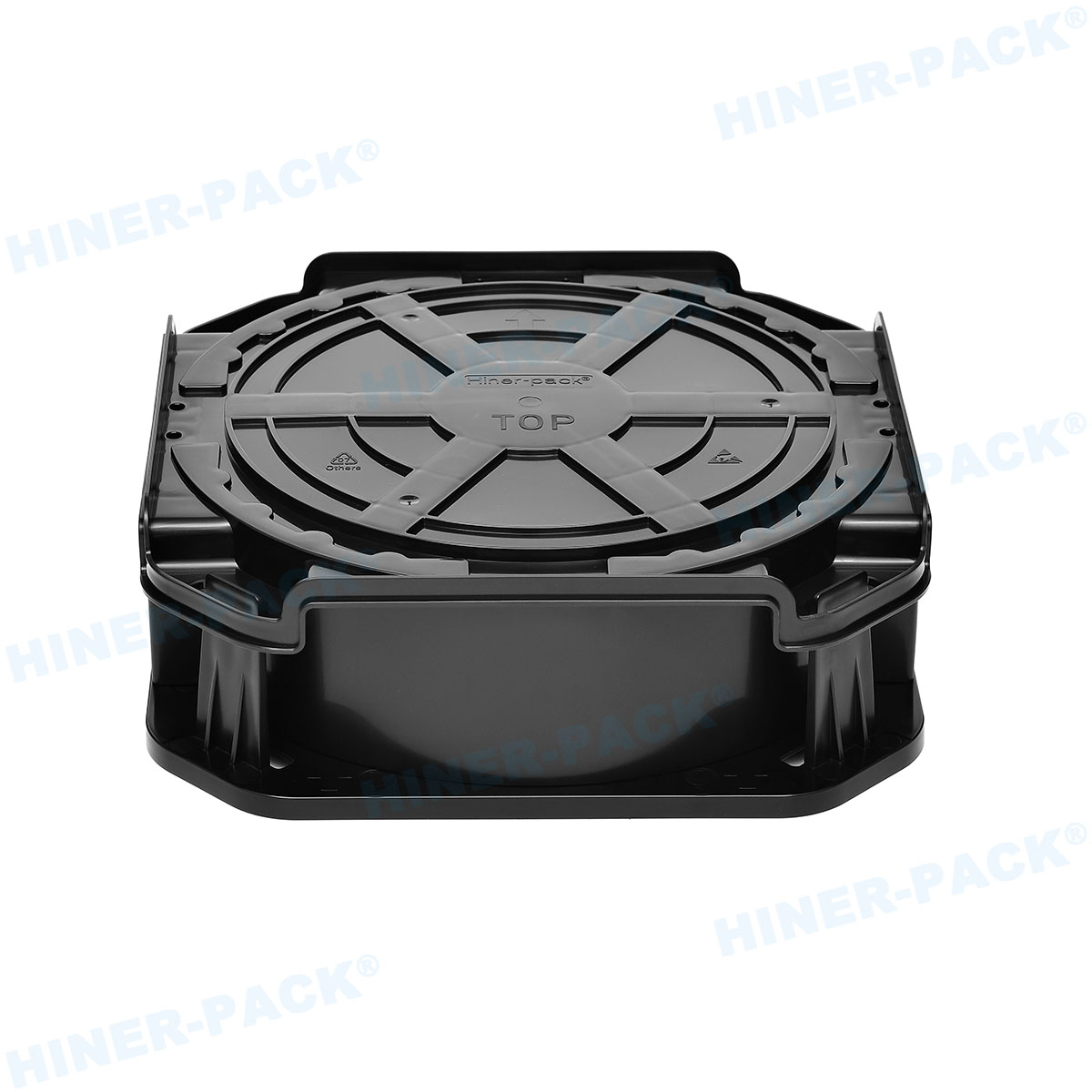
6. Summary of Engineering Trade-offs
When selecting wafer packaging, engineering teams must evaluate several competing parameters. The matrix below outlines how different performance characteristics influence production requirements and, consequently, the acquisition pricing of these containers:
| Canister Attribute | Standard Configuration | High-Performance Configuration | Impact on Manufacturing and Price |
|---|---|---|---|
| Material Base | Standard Polypropylene / Polystyrene | High-purity Polycarbonate / PEEK | High-performance polymers increase raw material expense but offer superior thermal and outgassing profiles. |
| ESD Protection | Surface anti-static coatings (migratory) | Carbon-fiber filled or inherently dissipative compounds | Permanent ESD protection requires complex compounding, which increases compound pricing. |
| Manufacturing Cleanliness | Standard industrial molding area | ISO Class 5 / 6 cleanroom molding and packing | Cleanroom operation and continuous air filtration increase overhead and unit production expenses. |
| Wafer Containment | Surface-contact cushions (foam/polystyrene) | Edge-grip non-contact retaining structures | Tight tolerances and multi-component assembly require precise molds and longer cycle times. |
By defining the minimum acceptable standards for particulate contamination and physical protection, packaging engineers can identify where they can standardise designs and where high-performance materials are required. This careful evaluation prevents over-engineering while securing the safe transit of finished and semi-finished silicon wafers across the global semiconductor supply chain.
Frequently Asked Questions
Q1: Why does a carbon-fiber-filled wafer canister have a higher price than a standard natural polypropylene carrier?
A1: Carbon-fiber-filled polycarbonate offers permanent ESD protection and high dimensional stability, which prevents structural deflection under thermal load. The raw carbon fiber additives and the specialized twin-screw compounding process required to disperse the fibers uniformly without generating loose particulates increase raw material expenses. Natural polypropylene is cheaper to produce but lacks built-in ESD protection and high structural rigidity.
Q2: How does the cleanroom rating of the packaging facility affect the final wafer canister price?
A2: Manufacturing wafer packaging in an ISO Class 5 or Class 6 cleanroom requires constant HEPA filtration, environmental monitoring, deionized water washing systems, and specialized operator apparel. The energy and maintenance overhead of these controlled environments adds to the manufacturing operational expenses, which is reflected in the final unit price of cleanroom-certified canisters compared to industrial-grade storage bins.
Q3: Can customized wafer thicknesses or slot configurations be accommodated, and how does this affect procurement?
A3: Yes, customized configurations for thinned wafers or automated handling systems are regularly developed. However, custom dimensions require new injection mold inserts, mechanical validation testing, and modifications to the molding parameters. These custom engineering steps and shorter manufacturing runs typically result in a higher unit price compared to off-the-shelf, high-volume standard canisters.
Q4: Do single-wafer coin shippers carry a different pricing structure than multi-wafer canisters?
A4: Yes, on a per-wafer basis, single-wafer shippers generally have a higher relative cost because they require dedicated, precision-molded internal shock-absorption components and specialized non-contact edge-grips for one individual substrate. Multi-wafer canisters distribute the packaging material volume and mold complexity across multiple wafers, making them more economical for high-volume bulk shipping.
Q5: What measures can procurement teams take to obtain the most competitive wafer canister price?
A5: Procurement teams can achieve better pricing by standardizing canister specifications across different product lines to consolidate purchase volumes. Committing to scheduled annual volume agreements allows manufacturers to run continuous production campaigns, which reduces setup overhead and lowers the per-unit price for the buyer.
For detailed inquiries regarding product specifications, customized configurations, or to request a formal quotation tailored to your production volume, please submit your specifications to our technical sales division at Hiner-pack. Our engineering team will assist in matching your wafer parameters with the appropriate packaging standards.














