
The global microelectronics industry relies on a highly complex and fragmented supply chain. Silicon substrates, epitaxial wafers, and processed device wafers frequently travel thousands of miles between fabrication facilities, packaging plants, and testing centers. Throughout this journey, these fragile discs of silicon, gallium nitride, or silicon carbide face severe mechanical and environmental hazards. Micro-cracks, surface particle contamination, electrostatic discharge, and organic outgassing represent constant threats to manufacturing yields. Consequently, selecting a specialized wafer box supplier is a fundamental decision that directly influences yield management and cost control.
For semiconductor manufacturers and packaging facilities, a transport container is not merely packaging; it is an extension of the cleanroom environment. The container must maintain its structural and chemical integrity under varying temperatures, pressures, and physical handling conditions. Evaluating a wafer box supplier requires a deep understanding of material science, precision engineering, and cleanroom contamination controls. This analysis explores the core engineering demands of wafer transport and establishes a framework for choosing a manufacturing partner capable of protecting high-value microelectronic substrates.
The Mechanical and Chemical Challenges of Substrate Transport
During transit, wafers are exposed to multi-directional forces and environmental shifts. Understanding these threats explains why standard industrial packaging is entirely inadequate for semiconductor transport.
Mechanical Shock and Structural Resonance
Logistical transport by road, air, or ocean introduces constant vibration and sudden impacts. If a wafer box lacks proper structural damping, these vibrations can transfer directly to the wafer edges. Silicon is inherently brittle, and compound materials like gallium arsenide are even more prone to fracture. Vibrations can cause wafers to collide with the internal slots of the carrier, leading to edge chipping, micro-fractures, or total breakage. A qualified wafer box supplier must design containers with precise tolerances and vibration-dampening geometries to isolate the substrates from external physical forces.
Electrostatic Accumulation and Discharge
Friction between the wafer and the carrier during transport generates electrostatic charges. If the packaging material is highly insulative, this charge accumulates, creating a high electrostatic potential. This phenomena leads to two major issues:
Electrostatic Attraction (ESA): The charged container surface acts as a magnet for airborne molecular contamination and microscopic particles, drawing them directly onto the active surface of the wafer.
Electrostatic Discharge (ESD): A sudden discharge of static electricity can instantly vaporize sub-micron metal lines and destroy gate oxides on processed wafers, rendering the integrated circuits non-functional.
Outgassing and Organic Contamination
Standard polymers often release volatile organic compounds (VOCs) over time, a process known as outgassing. When enclosed within a sealed shipping container, these volatile molecules settle onto the surface of the silicon. This thin layer of organic contamination can interfere with subsequent thin-film deposition, etching, or lithography steps, leading to device failure. Preventing outgassing requires the use of specialized high-purity engineering plastics and strict control over the manufacturing process.
Material Formulation and ESD Protection
The performance of a wafer transport container is fundamentally determined by the polymer formulation selected by the wafer box supplier. Specialized raw materials are compounded to balance mechanical strength, dimensional stability, chemical purity, and electrical properties.
Polycarbonate (PC) and Polypropylene (PP) Formulations
Polypropylene is widely used for cost-effective, durable shipping boxes. It provides excellent chemical resistance and flexibility, which helps absorb impacts. However, for applications requiring high dimensional stability, transparency for automated optical inspection, and superior temperature resistance, modified Polycarbonate is the industry standard. Polycarbonate offers high impact strength and minimal shrinkage during molding, ensuring that internal dimensions remain stable over years of use.
Carbon-Filled and Inherently Dissipative Polymers
To mitigate ESD hazards, suppliers compound base polymers with conductive additives. Carbon powder or carbon fiber is commonly integrated into the polymer matrix to lower surface resistivity into the static dissipative range, typically between 105 and 1011 ohms per square. Carbon nanotube (CNT) technology represents an advanced option, offering consistent electrostatic dissipation without the risk of carbon sloughing—a phenomenon where tiny carbon particles shed from the container and contaminate the wafers.
Outgassing Evaluation Standards
High-tier suppliers qualify their materials using standardized testing protocols, such as ASTM E595, which measures Total Mass Loss (TML) and Collected Volatile Condensable Material (CVCM). For advanced node manufacturing, materials must exhibit extremely low outgassing values to ensure that no molecular films deposit on active wafer surfaces during long-duration international shipping.
Key Categories of Wafer Shipping Containers
A capable wafer box supplier must provide a diverse portfolio of containers engineered for different wafer sizes, thicknesses, and automation requirements.
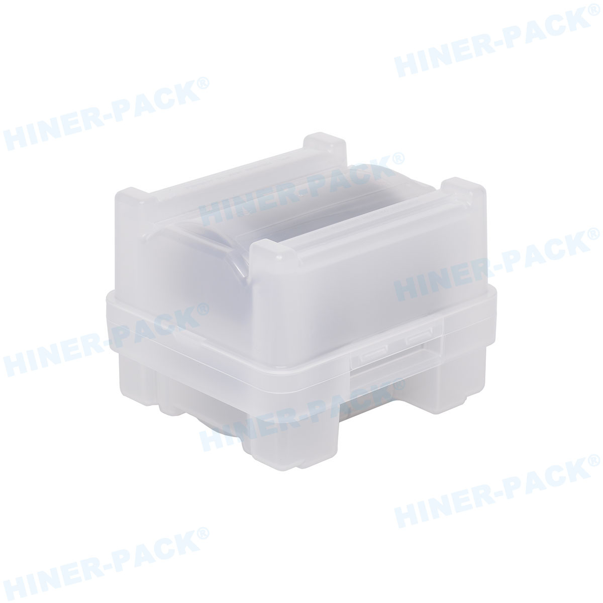
Coin-style shippers are designed for individual wafer transport, making them ideal for high-value research substrates, thin wafers, or compound semiconductor materials. These containers utilize a screw-on or snap-on lid configuration with internal spring cushions to immobilize the wafer, preventing lateral movement and surface contact.
Horizontal wafer shippers house multiple wafers stacked horizontally, separated by specialized lint-free interleaving pads. This design is highly effective for thin wafers (under 150 micrometers) that lack the structural rigidity to stand vertically without bowing. The horizontal support prevents gravitational sagging and reduces stress on the crystalline lattice.
Multi-wafer shipping boxes, designed to hold 25 wafers in a vertical orientation, are the standard for high-volume automated production. These boxes are engineered with precision-molded internal teeth or cassettes that grip each wafer securely at its perimeter. They must interface seamlessly with factory automated material handling systems (AMHS) and robotic end-effectors.
Cleanroom Manufacturing and Quality Control Processes
The manufacturing environment of a wafer box supplier is just as significant as the design of the box itself. Any contamination introduced during the injection molding process will ultimately find its way onto the wafer.
Precision Injection Molding in Controlled Environments
High-quality wafer carriers must be molded inside certified cleanrooms, typically ISO Class 5 or Class 6 environments. This setup ensures that airborne particulates do not become embedded in the molten polymer during the molding process, which could later flake off as particulate contamination.
Ultrasonic Deionized Water Washing
After molding, the components must undergo a multi-stage cleaning process. This sequence typically includes ultrasonic wash cycles using high-purity deionized (DI) water with a resistivity of 18.2 MΩ·cm. This process removes organic residues, ionic contaminants, and loose micro-particles. Following the wash, components are dried using hot, HEPA-filtered nitrogen or clean dry air (CDA).
Analytical Cleanliness Verification
Leading suppliers employ analytical testing to guarantee the cleanliness of their products. This testing includes:
Liquid Particle Counting (LPC): Measuring the size and concentration of particles extracted from the container surface to ensure compliance with strict cleanliness thresholds.
Ion Chromatography (IC): Detecting trace ionic contaminants, such as anions (chlorides, sulfates) and cations (sodium, ammonium), which can cause corrosion or electrical shifting on active semiconductor devices.
Gas Chromatography-Mass Spectrometry (GC-MS): Evaluating the outgassing potential of finished components under thermal stress to verify that no harmful organic vapors are released during transport.
Standardization and Robotic Compatibility
In automated fabs, dimensions must be accurate to the millimeter. Human operators rarely handle wafers directly; instead, robotic systems load and unload transport containers. Therefore, a wafer box supplier must design its products in strict accordance with SEMI (Semiconductor Equipment and Materials International) standards.
SEMI standards govern key parameters, including overall external dimensions, robotic pick-up notches, latch mechanisms, and cassette slot spacing. For 200mm and 300mm wafer processing, physical alignment features on the bottom of the box must align with kinematic pins on fab process equipment. A minor dimensional variation caused by poor mold maintenance or substandard resin selection can lead to robotic misalignments, wafer drops, and severe production downtime. Consequently, reliable suppliers implement automated optical inspection (AOI) systems on their production lines to measure every critical dimension before packaging.
Partnering with Hiner-pack for Substrate Protection
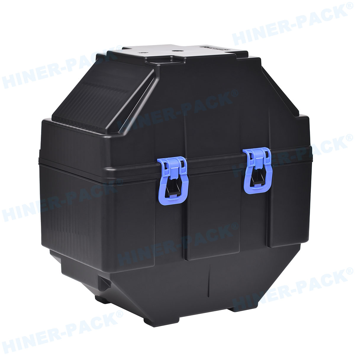
When selecting a supplier to secure your semiconductor supply chain, Hiner-pack delivers high-performance wafer transport solutions. Utilizing advanced engineering polymers, cleanroom injection molding, and comprehensive physical testing, Hiner-pack produces wafer containers that meet the stringent cleanliness and ESD standards of modern fabrication facilities. Our product lines support standard silicon, specialized compound semiconductors, and thin-wafer applications, ensuring that substrates arrive at their destination free from physical damage and chemical contamination. Through rigorous dimensional control and material purity testing, Hiner-pack acts as a reliable partner in protecting semiconductor yields across international logistics networks.
Frequently Asked Questions
Q1: What is the difference between antistatic, dissipative, and conductive materials in wafer packaging?
A1: Antistatic materials reduce the generation of static charges but do not safely bleed off existing charges. Dissipative materials have a surface resistivity between 105 and 1011 ohms per square, allowing static charges to flow safely to the ground at a controlled rate, preventing sudden ESD damage. Conductive materials have a resistivity below 105 ohms per square, which allows rapid charge transfer but can sometimes cause a sudden spark if a highly charged object makes contact.
Q2: Why is carbon nanotube (CNT) polymer technology preferred over carbon black powder?
A2: Carbon black powder is a cost-effective conductive additive, but under mechanical friction, carbon particles can slough off from the plastic matrix, creating conductive dust that contaminates wafers. Carbon nanotubes are structurally bound within the polymer matrix, providing consistent, uniform electrostatic dissipation without the risk of particle shedding.
Q3: How does a wafer box supplier ensure that shipping containers do not cause chemical outgassing?
A3: Suppliers manage outgassing by selecting raw engineering polymers that contain minimal volatile additives, plasticizers, or flame retardants. Additionally, the injection molding process parameters must be precisely controlled to prevent thermal degradation of the polymer, and finished boxes undergo vacuum baking or high-purity washing to remove surface-bound volatile organic compounds.
Q4: What SEMI standards are most applicable to wafer shipping boxes?
A4: Key standards include SEMI M1, which outlines physical specifications for silicon wafers; SEMI E1.9, which defines specifications for Front Opening Shipping Boxes (FOSB) used in 300mm wafer transport; and various standards governing the mechanical interfaces for robotic handling and automated material handling systems (AMHS).
Q5: Can wafer shipping boxes be reused, and what is the associated process?
A5: Yes, wafer shipping boxes can be reused if they are structurally intact and undergo a validated industrial cleaning process. This process involves disassembling the boxes, putting them through specialized multi-chamber washing machines utilizing deionized water and mild surfactant solutions, drying in a HEPA-filtered cleanroom environment, and verifying cleanliness via liquid particle counting before repackaging.
Secure Your Semiconductor Supply Chain
Selecting a reliable wafer box supplier is a decisive step in preserving the yield and reliability of your microelectronic components. The engineering team at Hiner-pack is ready to collaborate with your packaging and logistics specialists to design, test, and supply wafer containers tailored to your specific process tolerances and automation requirements. To request product samples, obtain engineering drawings, or receive a formal quotation for your upcoming wafer transport requirements, please contact our technical sales team directly to submit your inquiry.














