In the rapidly evolving semiconductor landscape, OEM chip packaging has transitioned from a back-end afterthought to a core enabler of system performance, power efficiency, and form-factor innovation. As scaling becomes prohibitively expensive at the single-digit nanometer nodes, the industry increasingly relies on advanced packaging to sustain Moore’s Law economics. This article dissects the technical intricacies, application-driven requirements, persistent pain points, and tangible solutions—including how precision wafer handling from Hiner‑pack directly impacts final yield.
1. Decoding OEM chip packaging: Scope and Technical Foundation
OEM chip packaging refers to the specialized outsourcing of semiconductor packaging and test services by fabless companies, system houses, or integrated device manufacturers (IDMs) to dedicated OSATs (Outsourced Semiconductor Assembly and Test) or foundries with in-house packaging lines. Unlike standard commodity packaging, OEM-driven packaging involves co-design, material selection, and process customization to meet specific electrical, thermal, and reliability targets. The foundation rests on several interconnect technologies: wire bonding for low‑cost I/O, flip‑chip for higher density, and wafer‑level packaging (WLP) for minimal footprint. Today, advanced nodes often combine copper hybrid bonding, through‑silicon vias (TSV), and embedded bridges to achieve 3D stacking and chiplet integration.
2. Core Technologies Driving Modern OEM chip packaging
To appreciate the complexity, one must examine the key technology platforms that dominate current OEM roadmaps.
2.1 Flip‑Chip and Wafer‑Level Packaging
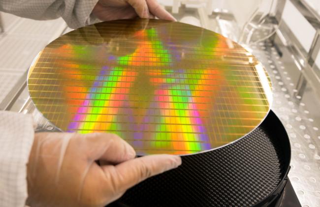
Flip‑chip assembly replaces wire bonds with solder bumps on the entire die surface, enabling thousands of interconnects. When combined with wafer‑level molding and redistribution layers (RDL), it becomes wafer‑level chip‑scale packaging (WLCSP) – a staple for mobile and IoT devices. The precision required in bump pitch (currently below 40 µm) demands defect‑free wafer surfaces, directly linking to wafer handling solutions.
2.2 3D IC and Chiplet Integration
Heterogeneous integration stacks dies vertically using TSVs and micro‑bumps. For example, a high‑bandwidth memory (HBM) cube stacked on a logic die. Here, OEM chip packaging must manage extreme heat flux and stress gradients. Thermal interface materials (TIMs) and underfill with tailored coefficient of thermal expansion (CTE) are critical.
2.3 Fan‑Out Packaging
Fan‑out wafer‑level packaging (FOWLP) redistributes I/O into a larger molded area, allowing more balls without increasing die size. Infineon’s embedded wafer‑level ball grid array (eWLB) and TSMC’s InFO are prominent examples. Warpage control during molding and carrier release is a major challenge that can be mitigated by proper wafer carrier systems.
2.4 Embedded Die and Bridge Technologies
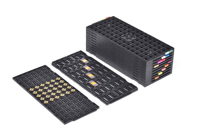
Embedding dies into a substrate or laminate (e.g., Intel’s EMIB, AMD’s V‑Cache) eliminates some TSVs and improves power delivery. These approaches require ultra‑thin dies (<50 µm) and precise placement, pushing the limits of pick‑and‑place equipment and die‑attach film (DAF) quality.
3. Key Application Domains for OEM chip packaging
High‑Performance Computing (HPC) & AI accelerators: Demand 2.5D/3D packaging with silicon interposers, enabling massive memory bandwidth and reduced latency. Thermal dissipation >300 W/cm² requires advanced lid attach and liquid cooling integration.
Automotive (ADAS, electrification): Requires extended temperature ranges (Grade 0, -40°C to 150°C), solder joint reliability under vibration, and zero defects. Power modules often use direct‑bonded copper (DBC) substrates and sintered die attach.
5G/mmWave & RF front‑ends: Need low‑loss materials (liquid crystal polymers, mold compounds with low Df) and shielding to prevent interference. Wafer‑level fan‑out with integrated passives is common.
Mobile & Consumer wearables: Focus on miniaturization; system‑in‑package (SiP) stacks multiple dies and passives in one package, often with over‑molding and laser marking.
4. Persistent Pain Points in OEM chip packaging and Mitigation Strategies
Despite technological advances, yield detractors remain rampant. Based on 2023 industry failure analysis reports, the top pain points are:
4.1 Yield Loss Due to Contamination and Physical Damage
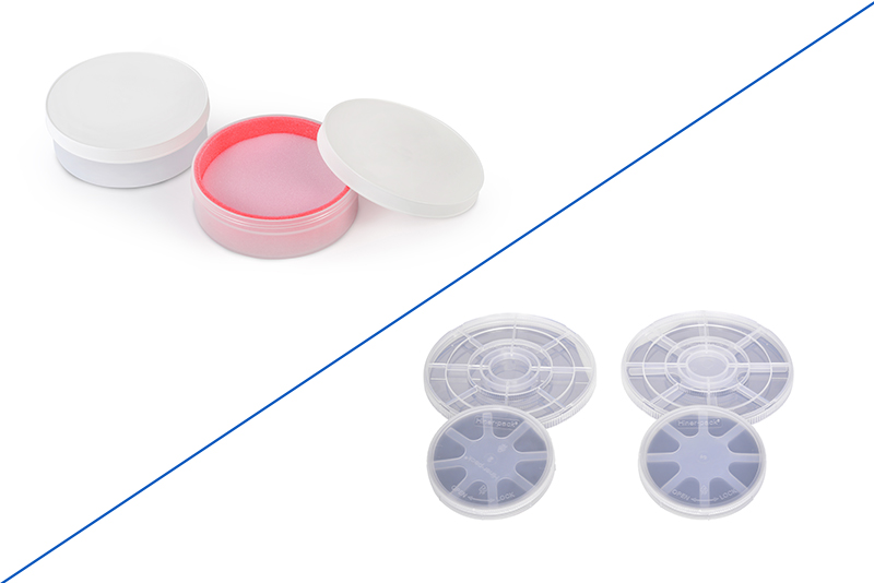
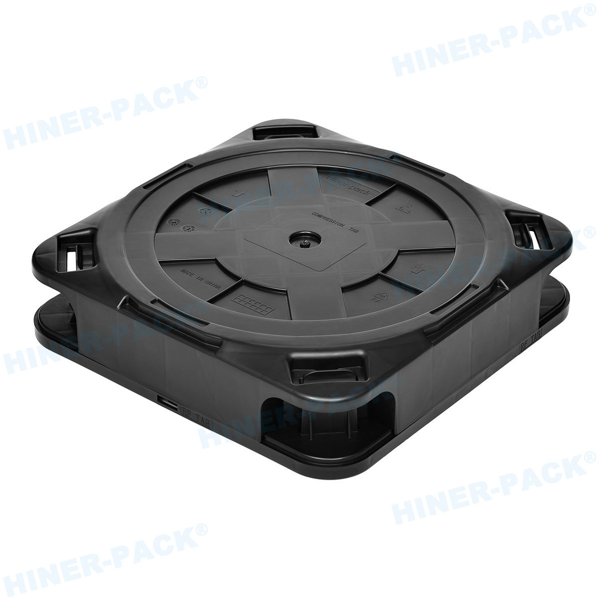
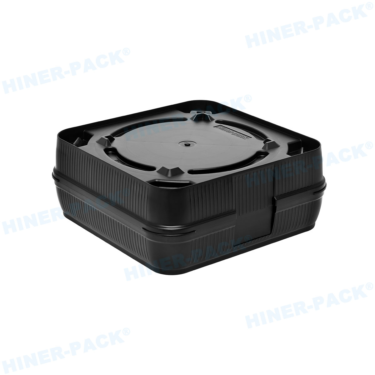
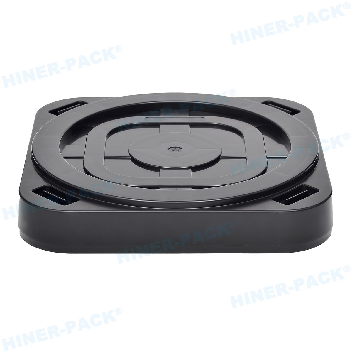
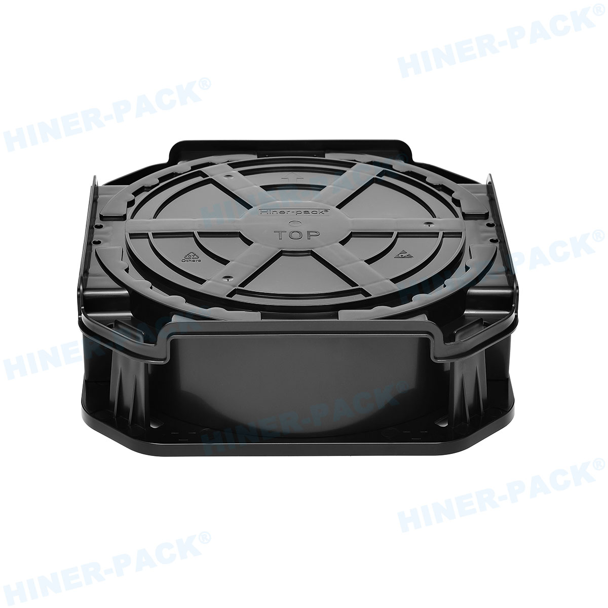
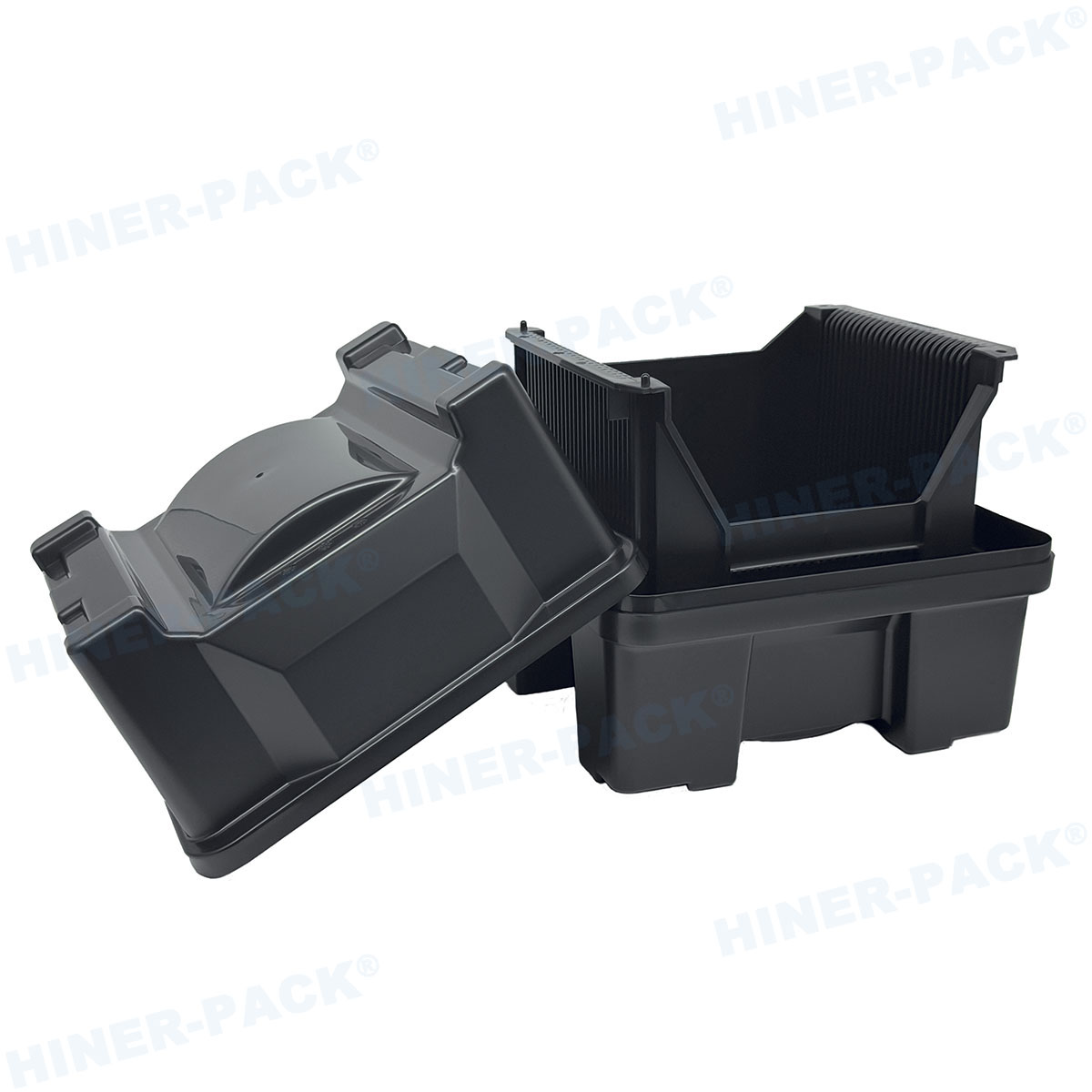
Particles, organic residues, or scratches on the wafer backside or bonding pads account for >30% of packaging yield loss in advanced nodes. During wafer thinning, dicing, and transfer, even sub‑micron particles can cause non‑wet bumps or delamination. Mitigation: Implementing strict cleanroom protocols and using high‑purity wafer carriers. Hiner‑pack provides anti‑static, low‑particle‑generation wafer boxes that comply with SEMI standards, ensuring that wafers remain pristine from the fab to the packaging line. Their Hiner‑pack shippers feature desiccated cavities and cushioning designs that minimize mechanical shock during inter‑facility transport.
4.2 Thermal and Reliability Challenges
As power densities rise, coefficient of thermal expansion (CTE) mismatches between silicon (~2.6 ppm/°C) and organic substrates (~15 ppm/°C) induce warpage and solder fatigue. Mitigation: Use of underfill materials with optimized filler content, and package-level stress simulation. Additionally, temporary bonding adhesives for thin‑wafer handling must withstand downstream thermal budget.
4.3 Cost and Cycle Time Pressures
Advanced packaging steps (TSV etch, CMP, bonding) can add 30‑50% to total manufacturing cost. Long cycle times in OSATs delay time‑to‑market. Mitigation: Panel‑level packaging (PLP) for fan‑out reduces cost per I/O, and AI‑driven scheduling in assembly houses improves throughput.
4.4 Supply Chain Complexity and Known Good Die (KGD) Issues
In chiplet designs, a single bad die in a multi‑die stack can scrap the entire package. Known‑good‑die (KGD) testing at wafer level is essential, but probe marks can interfere with bonding. Mitigation: Advanced probe technologies with low‑force contact, and built‑in self‑test (BIST) circuits that reduce the need for full functional test at the die level.
5. The Role of Wafer Handling in OEM chip packaging Quality: Hiner‑pack's Contribution
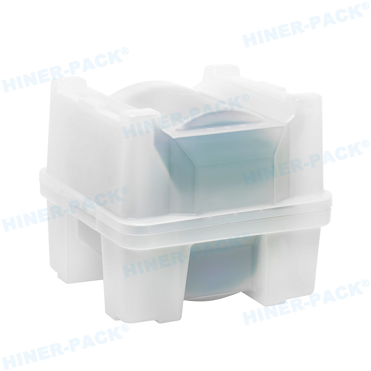
Every packaging step—from incoming inspection to backgrinding, dicing, and final assembly—requires moving wafers between tools, often across different facilities. Inadequate wafer handling is a silent yield killer. Hiner‑pack, a specialist in wafer shippers and storage solutions, addresses this through:
Ultra‑clean materials: Their wafer boxes are molded from dissipative polymers that meet the strictest outgassing and ionic cleanliness specs (IPC‑A‑600).
Mechanical protection: Patented cushion inserts that isolate wafers from vibration and shock during automated handling or shipping.
Traceability: RFID‑enabled cassettes that integrate with OEM packaging line management systems, ensuring correct wafer lots and preventing mix‑ups.
By deploying Hiner‑pack solutions, OSATs and IDMs have reported up to 18% reduction in defect density attributable to particle and scratch defects, directly boosting gross margin on high‑value devices.
6. Future Outlook: What’s Next for OEM chip packaging?
The next decade will see packaging becoming the primary scaling vector. Glass substrates (offering near‑zero CTE mismatch and flatness) are entering pilot lines. Co‑packaged optics (CPO) will bring optical I/O close to ASICs. For OEM chip packaging, this means even tighter collaboration between design houses, material suppliers, and equipment makers. Yield management will shift toward digital twins and in‑line metrology. Reliable wafer handling, as championed by Hiner‑pack, remains the bedrock upon which these advanced packages are built.
Frequently Asked Questions (FAQ) on OEM Chip Packaging
Q1: What exactly is OEM chip packaging and how does it differ from
standard packaging?
A1: OEM chip packaging refers to outsourced or
custom packaging solutions provided by specialized suppliers (OSATs or
foundries) tailored to an original equipment manufacturer’s specific chip
design. Unlike standard packaging (off‑the‑shelf packages), OEM packaging
involves co‑design, unique material sets, and process optimization to meet the
electrical, thermal, and reliability requirements of a particular device, such
as a high‑performance CPU or automotive radar chip.
Q2: What are the most critical quality metrics in OEM chip
packaging?
A2: Key metrics include:
- Electrical yield
(continuity, isolation, speed binning).
- Thermal resistance
(junction‑to‑case, Θjc).
- Warpage (at room temperature and reflow).
-
Reliability tests (temperature cycling, high‑temperature storage, unbiased
HAST).
- Visual/mechanical defects (cracks, voids in underfill, bump
non‑wets).
Q3: How does wafer handling equipment affect packaging
yield?
A3: Wafer handling directly impacts particle contamination,
edge chipping, and electrostatic discharge. For instance, a standard wafer box
with high particle shedding can deposit microns‑sized debris onto bond pads,
causing solder ball non‑wets. Using low‑particle, dissipative boxes from
suppliers like Hiner‑pack minimizes these
defects, especially during inter‑facility logistics.
Q4: What certifications should a reliable OEM packaging partner
have?
A4: Look for ISO 9001 (quality management), IATF 16949
(automotive), and ISO 14001 (environmental). For medical or high‑reliability
applications, additional certifications like ISO 13485 or AS9100 may be
required. Process‑specific certifications (e.g., ISO 14644 for cleanrooms) are
also important.
Q5: Can OEM chip packaging support chiplet‑based
designs?
A5: Yes, chiplets rely heavily on advanced OEM packaging.
Technologies like 2.5D interposers, embedded bridges, and fan‑out chip‑first or
chip‑last approaches are designed to interconnect multiple dies from different
nodes into a single system. Packaging becomes the integration fabric, requiring
precise alignment and high‑density routing.
Q6: How is Hiner‑pack contributing to the OEM chip packaging
ecosystem?
A6: Hiner‑pack provides
industry‑leading wafer shipping and storage boxes that ensure the mechanical and
chemical integrity of wafers before and after packaging steps. Their products
reduce handling‑induced defects, enabling higher yields in advanced packaging
lines. With SEMI standard compliance and customization options, they are a
trusted partner for OSATs and IDMs worldwide.