
Semiconductor manufacturing leaves zero room for error. A single damaged wafer, static discharge event, or microscopic dust particle can ruin high-value silicon, leading to millions of dollars in lost yield. Backend packaging and chip transport require total precision to keep vulnerable components intact.
Choosing a qualified wafer tray supplier directly impacts your final assembly yield and operational bottom line. At Hiner-pack, we develop specialized carrier solutions engineered to protect sensitive bare die and packaged integrated circuits (ICs) throughout complex global supply chains.
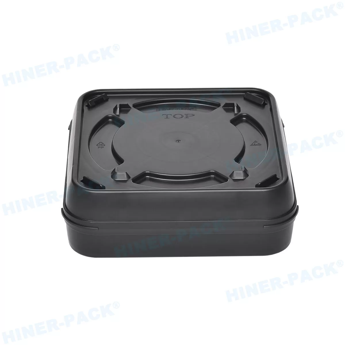
Types of Wafer Trays and Their Applications
Semiconductor devices come in diverse physical forms, requiring specific tray designs for safe transport, testing, and processing. Selecting the correct carrier format prevents physical damage and streamines automated handling.
Matrix Trays (JEDEC Standard Trays)
JEDEC standard matrix trays serve automated pick-and-place machines, surface-mount technology (SMT) lines, and automated test equipment (ATE). These trays feature standardized outer dimensions, allowing universal handling across different manufacturing equipment.
Their rigid grid pockets hold packaged ICs, BGAs, and QFNs in precise matrix formations. Uniform pocket spacing enables high-speed robotic vacuum nozzles to load and unload components without mechanical misalignments.
Pocket Trays / Bare Die Carriers
Bare die carriers and pocket trays protect exposed silicon dice and ultra-thin wafers that lack protective plastic or ceramic encapsulation. Active surface areas on bare dice remain highly sensitive to physical contact.
These specialized trays utilize recessed pocket steps and edge-only support features. The active die surface hangs freely in the cavity, preventing friction scratches and micro-cracks during long-distance shipping.
Waffle Packs & Coin Packs
Waffle packs and coin packs cater to low-volume chip handling, engineering validation, laboratory testing, and university research projects. A standard waffle pack consists of a grid matrix molded into a compact plastic tray, topped with paper inserts and static-dissipative foam.
Coin packs use circular stacking configurations to store small batches of silicon wafers or singulated dice safely during manual handling or low-volume processing steps.
Gel-Pak / Vacuum Release Trays
Fragile MEMS devices, GaAs chips, and ultra-thin bare dice require advanced non-pocket retention solutions. Gel-coated and vacuum release trays anchor chips in place using surface tension rather than rigid pocket walls.
During vacuum release, a vacuum applied underneath the tray lowers the gel's surface tension. This allows robotic pick-and-place tools to lift extremely delicate or non-standard die shapes without causing mechanical stress.
Critical Technical Factors When Evaluating a Supplier
Evaluating an enterprise-level wafer tray supplier requires deep technical due diligence. Minor variations in material composition or cavity tolerances can cause massive production line stoppages.
Material Selection
Plastics used in semiconductor packaging must maintain structural rigidity, thermal resistance, and chemical stability. Different applications demand specific high-performance polymers:
Polyethersulfone (PES): Offers exceptional dimensional stability and high thermal resistance, making it suitable for high-temperature baking processes up to 150°C.
Polyether Ether Ketone (PEEK): Delivers maximum mechanical strength, low wear rates, and excellent chemical resistance against aggressive solvent cleaning.
Conductive Polycarbonate (PC): Combines high impact strength with consistent static dissipation for general IC transport.
Acrylonitrile Butadiene Styrene (ABS): Provides a cost-effective material option for standard temperature transport and non-critical storage environments.
Carbon-Filled Material Blends: Integrate conductive carbon powder or fibers directly into the polymer matrix to create permanent electrostatic discharge paths.
ESD Protection (Surface Resistivity)
Electrostatic discharge (ESD) can destroy sensitive gate oxide layers in nanoseconds. Static electricity builds up naturally through triboelectric charging during transit, requiring continuous dissipation through the tray material.
Your wafer tray supplier must provide consistent surface resistivity across every pocket cavity. The industry-standard safe operating range spans between 104 and 109 ohms per square (ohms/sq):
Conductive Range (104 to 105 ohms/sq): Bleeds off static charges rapidly to ground, preventing high-voltage accumulation.
Static Dissipative Range (106 to 109 ohms/sq): Controls charge transfers at a slower, safer rate, avoiding sudden electrical arching.
Hiner-pack ensures static protection remains permanent. Our dissipative properties do not wash away with ambient moisture or degrade over time, fulfilling strict ANSI/ESD S20.20 standards.
Cleanroom Production & Outgassing
Particulate contamination ruins wire bonding pads and causes optical sensor defects. Wafer trays must be injection molded, inspected, and sealed inside certified ISO Class 5 or Class 6 (Class 100/1000) cleanrooms.
Outgassing occurs when volatile organic compounds (VOCs) escape from low-grade plastics under thermal or vacuum stress. These vaporized chemicals condense onto active die surfaces, creating invisible films that degrade high-frequency radio frequency (RF) chips and optical components. Technical buyers must insist on low-outgassing, virgin-grade polymers.
Dimensional Tolerance & Precision Cavities
Automated assembly machines run at extremely high speeds. Vacuum pick-and-place nozzles rely on consistent component positioning inside the tray grid.
A reliable supplier must maintain strict pocket tolerances, often as tight as ±0.05 mm. Loose tolerances allow the die to rotate, causing pick nozzles to misfeed. Tight tolerances clamp the die tightly, risking edge chipping under thermal expansion.
How to Qualify a Custom Wafer Tray Supplier
Procurement teams require a structured audit framework before onboarding a new packaging vendor. Use this practical checklist during your technical evaluation process.
Customization & Tooling Capabilities
Standard off-the-shelf trays rarely fit specialized bare die layouts. Verify whether the vendor provides complete custom tooling services:
In-house 3D CAD modeling and mechanical finite element analysis.
Rapid prototyping via precision CNC machining or 3D printing for fit testing.
Internal mold fabrication shop for rapid tooling production and modifications.
Specialized pocket designs with custom draft angles and corner relief radii.
Quality Certifications
Ensure your supplier maintains internationally recognized manufacturing standards. Crucial certifications include:
ISO 9001: Validates standardized quality management workflows across manufacturing facilities.
ISO 14001: Demonstrates compliance with environmental management and sustainable chemical handling.
RoHS & REACH Compliance: Guarantees products remain free from hazardous heavy metals and restricted chemical substances.
Quality Control (QC) Infrastructure
A reputable supplier must back their quality claims with advanced inspection equipment. Request proof of the following metrology tools in their quality assurance laboratory:
Coordinate Measuring Machines (CMM): For automated verification of pocket dimensions and surface flatness.
Surface Resistivity Meters: To test multi-point ESD performance across tray surfaces.
Liquid Particle Counters & Gas Chromatography: To measure residual particulate levels and verify low-outgassing properties.
Common Risks in Wafer Tray Sourcing & How to Avoid Them
Sourcing low-cost packaging materials without rigorous technical audits introduces serious operational hazards during chip shipping and assembly.
Die Migration and Flipping
Die migration occurs when chips jump out of their assigned pockets or flip upside down during air transport or road vibrations. This movement chips silicon edges, scratches active top-layer circuits, and jams automated feeder equipment.
Solution: Work with an experienced wafer tray supplier like Hiner-pack to engineer custom cover lids, internal retention clips, and interlocking tray stack designs that eliminate vertical pocket clearance.
Outgassing Contamination
Inexpensive recycled resins release microscopic chemical vapors during transit. These organic residues coat wire-bonding pads, leading to poor bond adhesion, high electrical resistance, and premature field failures in finished electronic devices.
Solution: Specify virgin-grade materials and require chemical composition certificates with every batch shipment to ensure total material purity.
Conclusion & Call to Action
Selecting the right semiconductor packaging partner is critical for yield optimization and risk reduction. Evaluating material grades, ESD stability, cleanroom standards, and pocket tolerances ensures your valuable silicon dies travel safely from backend processing to final packaging lines.
Hiner-pack combines advanced material science with precision cleanroom manufacturing to protect your semiconductors. Our engineering team designs custom matrix trays and bare die carriers tailored to your exact mechanical specifications.
Need custom wafer trays or standard matrix carriers for your next semiconductor project? Contact Hiner-pack today to request a free sample kit and a custom technical quote.
Frequently Asked Questions (FAQ)
Q1: What is the ideal surface resistivity range for ESD-safe wafer trays?
A1: The industry-standard surface resistivity for ESD-safe wafer trays ranges between 104 and 109 ohms/sq. Materials falling between 104 and 105 ohms/sq are conductive, while materials between 106 and 109 ohms/sq are static dissipative. Both ranges prevent sudden static discharges that destroy sensitive integrated circuits.
Q2: How do precise pocket tolerances impact automated packaging lines?
A2: Automated pick-and-place equipment requires strict pocket tolerances (typically within ±0.05 mm). Proper tolerances keep components perfectly centered, preventing robotic vacuum nozzles from missing picks, jamming assembly lines, or cracking delicate silicon edges.
Q3: Why is low outgassing critical for bare die carrier trays?
A3: Outgassing releases volatile organic compounds from low-grade plastics. These vapors settle onto unencapsulated silicon surfaces, creating micro-contaminants that ruin wire bonding adhesion, degrade optical lenses, and disrupt high-frequency radio frequency (RF) performance.
Q4: Can Hiner-pack design custom wafer trays for non-standard die dimensions?
A4: Yes. Hiner-pack provides full custom engineering services, including 3D CAD modeling, rapid prototyping, and precision mold tooling tailored to your exact die size, thickness, and pocket count requirements.
Q5: What is the difference between waffle packs and JEDEC standard matrix trays?
A5: Waffle packs feature compact grids designed for low-volume handling, engineering samples, and manual processing. JEDEC standard matrix trays follow strict standardized outer dimensions engineered for high-speed, fully automated SMT pick-and-place equipment and high-volume factory automation.














