For semiconductor fabrication and assembly facilities, the selection of a
wafer canister supplier directly influences process
stability, particle control, and overall device yield. Wafer canisters—also
referred to as wafer shipping boxes, FOUP (front opening unified pods)
alternatives, or wafer storage containers—serve as the primary environment for
wafer transfer between process steps, testing, and final packaging. This
analysis provides a structured framework for evaluating suppliers, covering
material science, cleanliness protocols, mechanical design, and logistics
integration.
Core Specifications That Define a Wafer Canister Supplier's Capability
The technical performance of wafer canisters rests on several interrelated
parameters. A competent wafer
canister supplier must demonstrate mastery across these dimensions
to meet the stringent requirements of modern semiconductor manufacturing.
Material Selection and Outgassing Control
Wafer canisters are predominantly manufactured from engineering
thermoplastics such as polycarbonate, polyetheretherketone (PEEK), or
static-dissipative polymers. The choice of base resin and additive package
determines critical properties including surface resistivity, mechanical
strength, and thermal stability. Outgassing—the release of volatile organic
compounds from polymer matrices—poses a significant contamination risk.
High-purity grades with low outgassing characteristics are mandatory for
advanced nodes (7nm and below). Suppliers that provide material certification
data, including ion chromatography and gas chromatography-mass spectrometry
results, enable fabs to verify compliance with cleanroom standards.
Beyond the base polymer, the surface finish of the canister interior requires
careful attention. Smooth, non-porous surfaces reduce particle adhesion and
facilitate cleaning cycles. Some suppliers offer specialized coatings or
fluoropolymer liners that further minimize friction and electrostatic discharge
(ESD) events during wafer insertion and extraction. When evaluating proposals,
request detailed material datasheets that specify melt flow index, flexural
modulus, and surface resistivity values measured under controlled
conditions.
Cleanliness and Particle Performance
Particle contamination remains one of the foremost yield detractors in
semiconductor processing. A wafer canister must maintain internal cleanliness
levels consistent with ISO Class 4 or better environments. This requires not
only pristine molding and assembly processes but also effective post-molding
cleaning procedures. Ultrasonic cleaning, deionized water rinsing, and nitrogen
purging are common steps in the manufacturing workflow of reputable
suppliers.
Qualification data should include particle shedding tests performed under
dynamic conditions—simulating the vibration and airflow experienced during
automated handling. Suppliers that conduct liquid particle counting (LPC) and
airborne particle counting (APC) on finished products provide verifiable
evidence of their cleanliness capabilities. Long-term storage tests, where
canisters are aged under accelerated conditions and then re-tested for particle
generation, offer additional assurance for high-reliability applications.
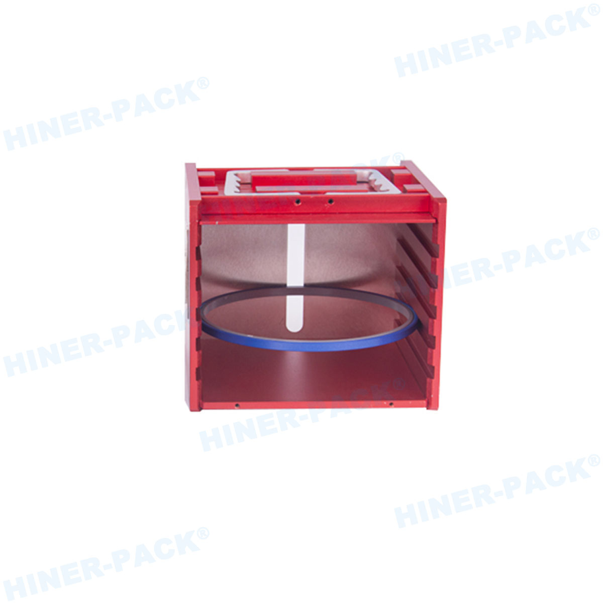
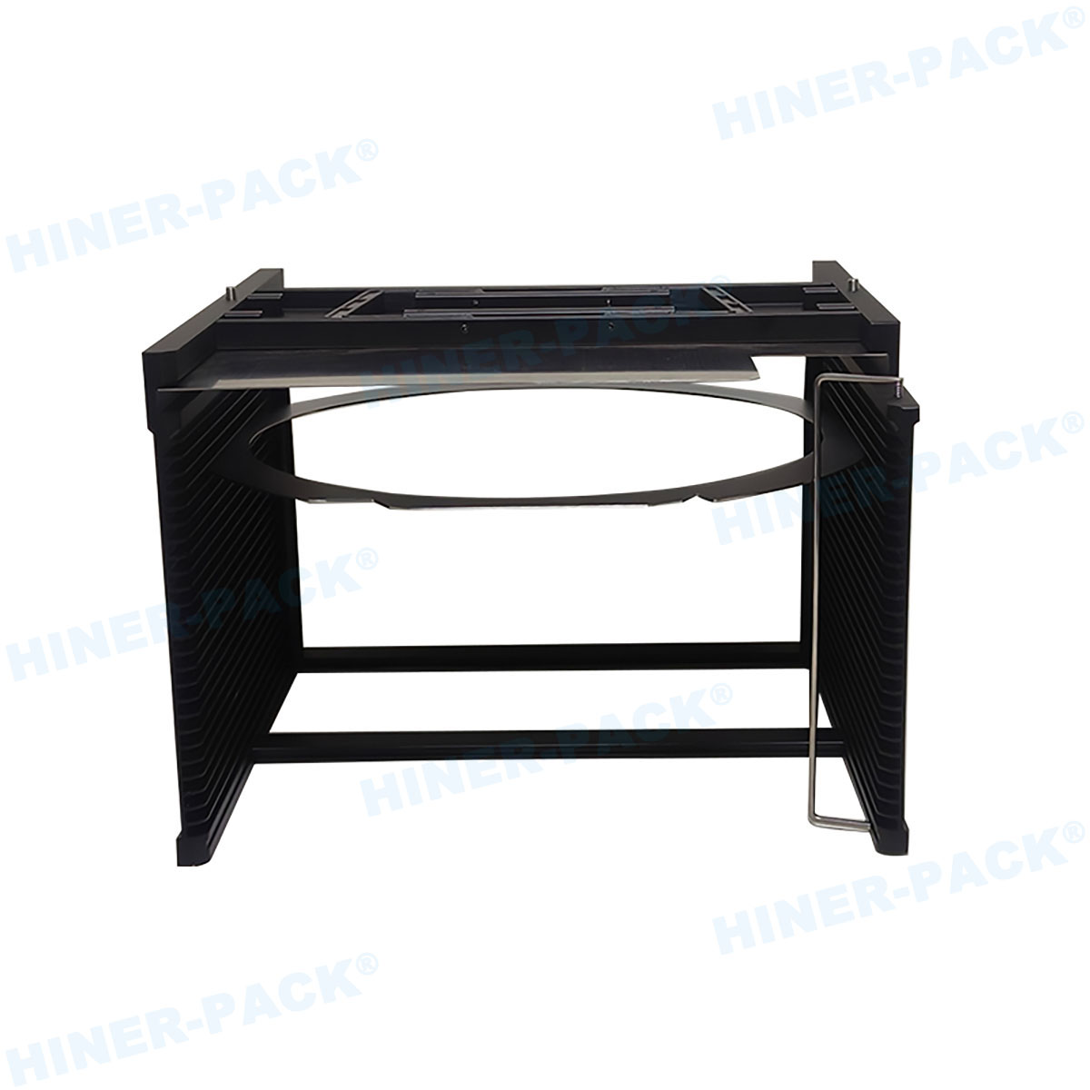
Mechanical Design and Wafer Protection
The mechanical architecture of a wafer canister determines its effectiveness
in protecting wafers from physical damage during transport and storage. Key
design features include:
Support structures that distribute wafer weight evenly, preventing bowing or
edge chipping.
Retention mechanisms that secure wafers without exerting excessive clamping
force.
Interlocking ribs or spacers that maintain minimum wafer-to-wafer gaps,
reducing contact risk.
Alignment features that enable precise docking with handling equipment
(robotic arms, AGVs).
Dimensional accuracy is equally important—canisters that deviate from SEMI
standard dimensions (e.g., SEMI E47 for 300mm FOUPs) can cause misalignment in
automated load ports. A reliable wafer
canister supplier provides detailed engineering drawings with
tolerances and performs CMM (coordinate measuring machine) inspections on every
production batch.
Operational Considerations in Supplier Selection
Beyond the product specifications, the operational capabilities of the
supplier affect day-to-day production efficiency. The following areas deserve
thorough evaluation during the vendor qualification process.
Supply Chain Reliability and Lead Times
Semiconductor fabs operate on tight production schedules, and any disruption
in canister availability can halt processing lines. Assess the supplier's
manufacturing capacity, raw material sourcing, and inventory management
practices. Suppliers with multiple production sites or safety stock agreements
offer greater resilience against supply shocks. Request historical data on
on-time delivery performance and average lead times for both standard and custom
configurations.
Traceability and Batch Control
Each wafer canister should carry unique identification markings (e.g.,
barcode, RFID) that enable full traceability from raw material receipt to final
shipment. This traceability supports root-cause analysis in case of
contamination events or quality deviations. Suppliers that implement statistical
process control (SPC) across their molding and cleaning operations can provide
batch-level trend reports, helping fabs monitor supplier performance over
time.
Logistics and Packaging for Inbound Shipments
The condition of canisters upon arrival at the fab depends heavily on the
supplier's packaging and shipping protocols. Double-bagging with nitrogen
backfill, desiccant packs, and shock-absorbent outer containers are standard
practices for maintaining cleanliness during transit. Verify that the supplier's
packaging meets your incoming inspection criteria and that they provide
certification of cleanliness upon request.
Application-Specific Requirements for Different Wafer Sizes and
Processes
Wafer canister specifications vary according to the diameter, thickness, and
processing history of the wafers being handled. 300mm wafers, with their larger
area and thinner profile, demand more robust support structures and careful
handling to prevent breakage. 200mm wafers, while more rigid, still require
clean environments to avoid defects. Additionally, wafers that have undergone
back-grinding or dicing require canisters with modified interior geometries to
accommodate reduced thickness or singulated die.
Some processes, such as copper pillar bumping or fan-out wafer-level
packaging (FOWLP), involve elevated temperature steps that may require canisters
with higher heat deflection temperatures. Suppliers that offer material
formulations optimized for these conditions demonstrate a deep understanding of
the semiconductor packaging ecosystem. Hiner-pack provides product families tailored to specific wafer diameters and process
stages, ensuring that each canister design aligns with the mechanical and
thermal demands of the application.
Quality Management Systems and Certification
An experienced wafer
canister supplier operates under established quality management
frameworks. ISO 9001 certification is a baseline requirement, but
semiconductor-specific standards such as IATF 16949 (automotive) or ISO 13485
(medical) may be relevant if the final devices serve those sectors. More
importantly, the supplier should demonstrate adherence to SEMI standards and
participation in industry working groups—this indicates engagement with the
evolving requirements of the semiconductor community.
On-site audits provide the most reliable assessment of a supplier's quality
culture. During audits, examine incoming material inspection records, in-process
control charts, final test data, and non-conformance handling procedures.
Suppliers that maintain comprehensive documentation and readily share quality
metrics tend to deliver consistent product performance over the long term.
Integration with Factory Automation Systems
Modern wafer fabs rely on material handling systems (MHS) that transport
canisters between tools, stockers, and test equipment. The canister's physical
interface—including mechanical latching, RFID antenna placement, and optical
alignment targets—must be compatible with the fab's automation infrastructure.
Suppliers should provide detailed dimensional data and interface specifications
to support integration testing. Some suppliers offer engineering services to
customize canister features for specific load ports or transfer systems,
reducing the risk of jams or misalignment during high-speed operation.
Furthermore, the canister material must not interfere with automated
identification systems—for instance, RF-blocking polymers can hinder read/write
operations. Suppliers that conduct RF compatibility tests and provide guidance
on antenna placement help fabs avoid integration pitfalls. Hiner-pack offers technical consultation to ensure seamless integration with existing fab
infrastructure, from load ports to stockers.
Supplier Collaboration and Technical Support
Selecting a wafer canister supplier extends beyond a transactional
purchase—it initiates a technical partnership. Suppliers that assign dedicated
application engineers to support customers offer advantages in troubleshooting,
process optimization, and new product introduction. During the evaluation phase,
assess the supplier's responsiveness to technical inquiries, their willingness
to conduct joint experiments, and their track record of resolving field
issues.
Suppliers that maintain test labs with particle counters, surface analyzers,
and environmental chambers can perform custom testing to simulate your specific
handling conditions. This collaborative approach reduces uncertainty and
accelerates qualification timelines.
Frequently Asked Questions About Wafer Canister Supplier Selection
Q1: What certifications should a wafer canister supplier
hold?
A1: At minimum, ISO 9001 certification for quality
management. For advanced applications, look for suppliers that comply with SEMI
standards (e.g., SEMI E47, E62) and hold additional certifications such as IATF
16949 if the end products serve automotive markets. Cleanliness certifications
per ISO 14644 are also valuable.
Q2: How does a wafer canister supplier control particle
contamination?
A2: Reputable suppliers employ a combination of material
selection (low-outgassing polymers), precision molding in clean environments,
ultrasonic cleaning, deionized water rinsing, and nitrogen purging. They also
conduct particle shedding tests under dynamic conditions and provide cleanliness
certification with each shipment.
Q3: What is the difference between a FOUP and a wafer
canister?
A3: FOUP (front opening unified pod) is a specific type of
wafer canister standardized for 300mm wafers with a front-opening interface. The
term "wafer canister" encompasses a broader range of containers—including
side-opening boxes, shipping trays, and custom carriers for 200mm or smaller
wafers. The supplier should clarify which standard their product follows.
Q4: Can a wafer canister supplier provide custom designs for
non-standard wafer sizes or processes?
A4: Yes, many suppliers offer engineering services to
modify interior geometries, material formulations, or interface features.
Customization may be required for wafers with patterned edges, thin profiles, or
specific handling requirements. Discuss your process needs early to determine
the feasibility and lead time for custom solutions.
Q5: How often should wafer canisters be requalified in the fab
environment?
A5: Requalification frequency depends on usage intensity
and cleaning cycles. Typically, canisters undergo visual inspection and particle
testing after a certain number of cycles (e.g., 50 or 100 uses). Suppliers can
recommend requalification intervals based on their material durability testing.
Regular monitoring of incoming cleanliness levels also helps determine when
requalification is needed.
Q6: What logistics factors should I consider when choosing a wafer
canister supplier?
A6: Evaluate the supplier's packaging for inbound
shipments—double-bagging, nitrogen backfill, and shock protection are important.
Also assess their lead times, safety stock levels, and ability to provide
emergency replenishment. Suppliers with regional distribution centers can reduce
shipping delays and simplify customs clearance.
Request a Comprehensive Wafer Canister Supplier Qualification Package
Selecting the optimal wafer
canister supplier requires careful analysis of technical
specifications, operational capabilities, and long-term support. Hiner-pack specializes in engineered wafer handling solutions that meet the rigorous
demands of semiconductor packaging—from front-end fabs to back-end assembly.
Our engineering team provides detailed product documentation, including
material datasheets, cleanliness validation reports, and dimensional inspection
certificates. We offer on-site technical support for integration and
qualification, ensuring that our canisters perform consistently in your
production environment.
To receive a tailored proposal and technical portfolio for your specific
wafer dimensions and process requirements, please contact our semiconductor
packaging specialists through the Hiner-pack website. We welcome detailed
inquiries and confidential discussions regarding your wafer handling
challenges.


