For semiconductor manufacturing teams, three distinct perspectives often
emerge when assessing wafer canister suppliers: the technical parameter
checklist (Top 5 Technical Parameters That Define a High-Performance Wafer
Canister Manufacturer), the differentiation question (What
Distinguishes a Premium Wafer Canister Manufacturer from Standard
Suppliers?), and the yield impact consideration (Achieving
Contamination-Free Transport: The Wafer Canister Manufacturer's Impact on
Yield). This examination addresses all three through a detailed technical
lens, focusing on material science, precision engineering, and contamination
control—the pillars that separate commodity suppliers from true partners in
semiconductor production.
The selection of a wafer
canister manufacturer directly influences front-end and back-end
yield rates, particularly as device geometries shrink and packaging
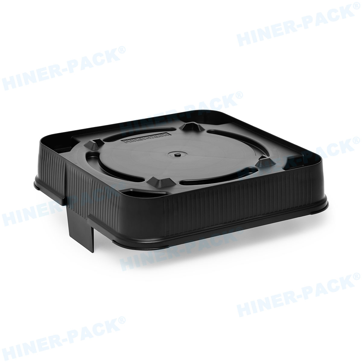
architectures become more complex. A wafer canister—often referred to as a wafer
carrier or shipping box—serves as the primary protective enclosure for silicon
wafers during storage, inter-facility transport, and tool load/unload
operations. Beyond simple mechanical protection, modern canisters must maintain
stringent environmental conditions, minimize particle generation, and ensure
electrostatic discharge (ESD) safety. Companies like Hiner-pack have
established specialized production lines addressing these multilayer
requirements, integrating cleanroom molding, precision metrology, and
lot-traceable quality systems.
This article systematically examines the technical attributes that define a
high-caliber wafer canister manufacturer, from polymer chemistry and mold design
to cleanroom protocols and supply-chain quality assurance. Each section builds
upon the preceding one, creating a comprehensive framework for technical
evaluation.

Material Science as the Foundation of a Wafer Canister Manufacturer's
Offering
The material selection process represents the first and most consequential
decision a wafer
canister manufacturer makes. Polymers used in wafer canisters must
satisfy a demanding set of physical, chemical, and electrical properties
simultaneously—a combination rarely found in off-the-shelf engineering
plastics.
Polymer Selection Criteria
High-performance wafer canisters typically employ semi-crystalline
thermoplastics such as polyetheretherketone (PEEK), polyetherimide (PEI),
polyphenylene sulfide (PPS), or polycarbonate (PC). Each polymer family offers
distinct trade-offs:
PEEK provides exceptional thermal stability (continuous use
up to 260°C), chemical resistance, and mechanical strength, making it suitable
for high-temperature processes and aggressive cleaning agents.
PEI offers excellent dimensional stability and inherent
flame retardance, with glass transition temperatures around 217°C, well suited
for automated handling systems requiring repeated thermal cycling.
PPS delivers outstanding chemical resistance and low
moisture absorption, particularly valuable in wet processing environments where
hydrolysis resistance is paramount.
PC provides optical clarity and good impact resistance at a
lower cost point, though its use is typically restricted to less demanding
applications or single-use scenarios.
The choice of base polymer directly affects the canister's ability to
maintain wafer flatness, resist creep under stacked loads, and survive repeated
autoclave or vapor-phase sterilization cycles. A competent wafer canister
manufacturer conducts extensive material characterization, including
differential scanning calorimetry (DSC), thermogravimetric analysis (TGA), and
dynamic mechanical analysis (DMA), to validate material performance across the
intended operational temperature range.
Antistatic Properties and Surface Resistivity
Wafer damage from electrostatic discharge (ESD) remains one of the most
common yet preventable failure modes in semiconductor handling. The wafer
canister manufacturer must engineer surface resistivity within the range of
106 to 1011 Ω/sq—sufficiently conductive to dissipate
static charges without being so conductive as to create shorting paths. This is
achieved through either:
Intrinsic dissipative polymers that incorporate conductive
fillers (carbon nanotubes, graphene, or metal-coated particles) uniformly
distributed throughout the resin matrix.
Surface coatings or additives applied during molding or as
a post-process treatment, though these can introduce contamination risks and
wear-related degradation over time.
The more sophisticated approach involves compounding custom masterbatches
with precisely controlled filler loadings, ensuring consistent dissipation
performance across all canister walls and features. A reputable wafer canister
manufacturer validates ESD performance through surface resistivity measurements
per ASTM D257 and static decay testing per ANSI/ESD S11.11, providing
batch-level certification data to customers.
Outgassing and Extractables Control
Volatile organic compounds (VOCs) and ionic extractables released from
canister materials can condense onto wafer surfaces, forming haze, organic
contamination, or corrosion sites that degrade device performance. The wafer
canister manufacturer addresses this through:
Selection of low-outgassing grades of base polymers, often certified to NASA
low-outgassing specifications (ASTM E595).
Optimization of molding parameters (melt temperature, residence time,
injection pressure) to minimize polymer degradation and additive
decomposition.
Post-molding extraction processes, such as supercritical CO2 cleaning or ultrasonic rinsing in deionized water, to remove residual monomers,
oligomers, and processing aids.
Analytical verification using gas chromatography-mass spectrometry (GC-MS)
and ion chromatography (IC) provides quantitative data on outgassing species and
extractable ion levels, enabling the wafer canister manufacturer to certify
cleanliness to ISO 14644-1 Class 3 or better standards.
Precision Engineering in Wafer Canister Design
Material properties alone cannot guarantee wafer protection; the geometric
design and manufacturing precision of the canister are equally critical.
Engineering decisions made by the wafer canister manufacturer influence
everything from robotic handling reliability to stack density in automated
storage systems.
Dimensional Tolerances and Automation Compatibility
Modern semiconductor fabs operate with fully automated material handling
systems (AMHS) that transfer wafer canisters between process tools, stockers,
and load ports. These systems rely on precise kinematic coupling between the
canister and end-effectors, requiring:
Critical dimensions (outer profile, handle geometry, and alignment features)
held to tolerances of ±0.1 mm or better.
Flatness of the wafer support surface within 0.05 mm across the entire
wafer-contact area to prevent wafer warpage.
Consistent centerline and orientation key positions to ensure repeatable
engagement with tool load ports.
A premium wafer canister manufacturer employs multi-axis coordinate measuring
machines (CMM) and optical comparators for 100% inspection of critical features,
with statistical process control (SPC) charting to detect dimensional drift
early. This level of precision enables seamless integration with both legacy 200
mm and next-generation 300 mm and 450 mm handling platforms.
Sealing Mechanisms and Environmental Isolation
Wafer canisters must maintain a controlled internal environment—typically dry
nitrogen purge or clean dry air—to prevent oxidation, moisture adsorption, and
particle ingress. The sealing system comprises:
An elastomeric gasket or O-ring seated in a precisely machined groove on the
canister body or lid.
A clamping or latching mechanism that applies uniform compressive force
around the seal perimeter.
Optional pressure-relief or purge ports for active gas flow during
storage.
The wafer canister manufacturer must balance seal compression against ease of
opening, ensuring that automated or manual operators can access wafers without
excessive force that could generate particles. Finite element analysis (FEA) of
seal deformation and contact pressure guides the design of both the seal
geometry and the latching system, achieving leak rates below 1 × 10⁻⁶ Pa·m3/s as measured by helium leak detection.
Stacking Configurations for Storage Efficiency
Wafer canisters are frequently stacked in storage racks or shipping
containers, requiring robust structural design that supports the weight of
multiple loaded units without distortion. Key engineering considerations
include:
Reinforced corners and ribs that distribute stack loads away from wafer
support areas.
Interlocking features between stacked canisters to prevent lateral shifting
during transport.
Stress-relief radii in high-load areas to avoid stress cracking over
extended use cycles.
Through accelerated life testing—including vibration, drop, and compressive
creep tests—the wafer canister manufacturer validates stack performance under
real-world logistics conditions, providing customers with certified stack height
limits and load ratings.
Particle Control Across the Manufacturing and Supply Chain
Particles remain the single largest yield detractor in semiconductor
manufacturing, and the wafer canister represents a potential source of both
intrinsic and extrinsic contamination. A disciplined wafer
canister manufacturer implements comprehensive particle control
measures throughout the production and logistics chain.
Cleanroom Manufacturing Standards
Injection molding, the primary manufacturing process for wafer canisters,
inherently generates particles through resin friction, mold wear, and material
handling. To mitigate this, the wafer canister manufacturer operates molding
cells within ISO 14644-1 Class 5 (Class 100) or cleaner cleanrooms, with:
High-efficiency particulate air (HEPA) or ultra-low penetration air (ULPA)
filtration providing 0.3 μm particle removal efficiency of 99.97% or
better.
Positive-pressure cleanroom environments to prevent external contamination
ingress.
Strict gowning protocols and material transfer procedures for all personnel
and incoming raw materials.
Advanced manufacturers employ cleanroom-compatible injection molding machines
with sealed hydraulic systems, ceramic-coated barrels, and minimized moving
parts to reduce internal particle generation. In-line particle counters monitor
airborne particle concentrations in real time, triggering alarms if levels
exceed predefined control limits.
Post-Molding Cleaning Processes
Even under cleanroom molding conditions, molded parts require post-processing
cleaning to remove residual particulates, mold-release agents, and surface
contaminants. Common cleaning sequences include:
Ultrasonic cleaning in deionized water with surfactant additives, followed
by multiple rinse stages.
Isopropyl alcohol (IPA) or ethanol vapor degreasing for organic residue
removal.
Pressurized air or nitrogen blow-off with ionized gas to neutralize static
charges and dislodge adhered particles.
Cleaning efficacy is verified using particle extraction tests, where cleaned
canisters are filled with ultrapure water or solvent, agitated, and the rinse
fluid is analyzed for particle count and size distribution (typically down to
0.1 μm) using liquid particle counters. A high-quality wafer canister
manufacturer achieves extractable particle levels below 100 particles per
milliliter at 0.1 μm threshold.
Packaging and Transport Protocols
After cleaning, wafer canisters must be packaged to maintain cleanliness
through storage and shipment. Double-bagging with ESD-safe, low-particulate
films, often with vacuum sealing or nitrogen flushing, prevents recontamination.
The packaging process itself occurs in a cleanroom environment, with:
Automated bagging equipment to minimize human contact and particle
shedding.
Heat sealing with controlled temperature and pressure to ensure bag
integrity.
External carton packaging with cushioning materials that do not shed fibers
or generate static charge.
For international shipments, the wafer canister manufacturer must also
consider climate control—desiccant packs or humidity indicators may be included
to prevent moisture condensation during temperature fluctuations, which could
lead to water spot formation on wafers.
Application-Specific Requirements for Wafer Canisters
Different semiconductor applications impose unique demands on wafer canister
design and performance. A versatile wafer canister manufacturer offers product
families tailored to specific use cases, rather than a one-size-fits-all
approach.
300mm Wafer Handling
The transition to 300mm wafers introduced new challenges due to increased
wafer weight, larger surface area, and higher device count per wafer. Canisters
for 300mm wafers—often complying with SEMI E15 standards—feature:
Enhanced structural rigidity to support the greater weight of 300mm wafers
(approximately 2.5 kg per 25-wafer lot).
Redesigned wafer support ribs that minimize contact area while providing
uniform support across the wafer backside.
Side- or top-loading configurations compatible with 300mm tool load ports
and industry-standard FOUP (front opening unified pod) interfaces.
For advanced nodes (7nm and below), additional considerations include
ultra-low particle generation (down to 0.05 μm) and extremely low volatile
outgassing to prevent contamination of sensitive gate stacks and interconnect
layers.
Advanced Packaging Applications
Wafer-level packaging (WLP), fan-out wafer-level packaging (FOWLP), and 3D
integration technologies often involve thinned wafers (50-100 μm thickness) that
are highly fragile and susceptible to warpage. Canisters designed for these
applications incorporate:
Reduced clamping forces and distributed support to avoid stress-induced
cracking in thin wafers.
Precise temperature control features (e.g., thermal mass or insulation) to
minimize thermal cycling stress during storage between process steps.
Compatibility with temporary bonding and debonding carriers, allowing
seamless transfer between handling and processing equipment.
The wafer canister manufacturer collaborates with packaging engineers to
understand specific warpage profiles and stress sensitivities, customizing
canister geometry to match the unique mechanical behavior of each wafer
type.
Thin Wafer and Sensitive Device Transport
Beyond packaging, applications involving compound semiconductors (GaAs, GaN,
SiC), MEMS devices, or optical components require additional protective
measures:
Internal dividers or individual wafer slots with soft contact materials to
prevent surface scratching.
Light-blocking or UV-resistant canister materials for photonic devices
sensitive to ambient light.
Hermetic sealing options for moisture-sensitive or oxygen-sensitive
materials, with integrated getter materials to absorb residual gases.
These specialized requirements demand engineering flexibility and willingness
to develop non-standard solutions—a hallmark of a responsive and technically
capable wafer canister manufacturer.
Quality Assurance Protocols in Wafer Canister Production
Consistency across production lots is essential for semiconductor customers
who run high-volume manufacturing with tightly controlled processes. The wafer
canister manufacturer must deploy rigorous quality assurance (QA) systems that
detect and eliminate variability at every stage.
Inspection and Testing Standards
Comprehensive inspection protocols cover both dimensional and cleanliness
attributes:
Dimensional inspection: Automated optical inspection (AOI)
systems capture critical dimensions, flatness, and surface defects at speeds
matching production rates.
Particle testing: Liquid particle extraction, as described
earlier, is performed on a sampling basis per lot, with statistical sampling
plans (e.g., ANSI/ASQ Z1.4) defining sample sizes and acceptance criteria.
ESD testing: Surface resistivity and charge dissipation are
verified using standardized methods, with calibration traceable to national
standards.
Mechanical testing: Stack load capacity, latch cycle life,
and impact resistance are validated through periodic destructive
testing.
A premium wafer canister manufacturer maintains a metrology laboratory with
calibrated instruments and documented test procedures, ensuring measurement
reproducibility across shifts and production lines. Hiner-pack implements these protocols with a focus on data integrity and traceability,
providing customers with detailed inspection reports upon request.
Batch Traceability and Documentation
Traceability from raw material receipt to finished goods shipment enables
rapid root-cause analysis in the event of a quality excursion. Key traceability
elements include:
Unique lot numbers assigned to each batch of resin, with certificates of
analysis (CoA) and material safety data sheets (MSDS) on file.
Machine-level tracking of molding parameters (temperature, pressure, cycle
time) for each production run.
Serialized labeling of individual canisters or boxes, allowing customers to
correlate field performance with specific production conditions.
This traceability framework supports both internal quality improvement
initiatives and external customer audits, providing transparency into the
manufacturing process that reinforces trust.
Consistency Validation Across Production Lots
Statistical process control (SPC) charts monitor key quality characteristics
over time, detecting shifts or trends before they lead to non-conformances. The
wafer canister manufacturer uses:
Control charts (X-bar and R, or X-bar and S) for critical dimensions and
particle counts.
Process capability indices (Cpk, PpK) to quantify the ability of processes
to meet specification limits.
Periodic gauge repeatability and reproducibility (R&R) studies to ensure
measurement systems remain capable.
By maintaining process stability and capability, the wafer canister
manufacturer delivers consistent product quality that minimizes incoming
inspection overhead for customers and reduces the risk of process
disruptions.
Evaluating a Wafer Canister Manufacturer's Technical Capabilities
When selecting a wafer
canister manufacturer, semiconductor companies should assess not
only product specifications but also the supplier's underlying technical
infrastructure and innovation pipeline. The following dimensions provide a
framework for comparative evaluation.
Research and Development Investment
Semiconductor technology evolves rapidly, with new materials, device
architectures, and process conditions emerging constantly. A forward-looking
wafer canister manufacturer maintains an active R&D program that
includes:
Materials research to evaluate novel polymers, fillers, and surface
treatments for next-generation requirements.
Design optimization using computational fluid dynamics (CFD) and FEA to
improve cleanliness, airflow, and mechanical performance.
Collaboration with equipment suppliers and research consortia to stay ahead
of industry roadmaps (e.g., IEEE International Roadmap for Devices and
Systems).
Evidence of R&D activity can be seen in patent filings, technical
publications, and participation in industry standards committees. These
indicators suggest that the wafer canister manufacturer is not merely reacting
to current specifications but actively shaping future capabilities.
Customization and Engineering Support
No two semiconductor fabs are identical, and off-the-shelf canister designs
may not address specific handling constraints, tool interface requirements, or
cleanroom protocols. A responsive wafer canister manufacturer offers engineering
services that include:
Customized dimensional configurations to fit non-standard storage racks or
load ports.
Modified latching or sealing systems for unique automation interfaces.
Special material formulations to address specific chemical compatibility or
thermal requirements.
These customizations require both design expertise and production
flexibility, including the ability to modify mold tooling or run small-batch
pilot production. A wafer canister manufacturer with in-house tool-making and
prototyping capabilities can deliver custom solutions with shorter lead times
and lower engineering costs.
Production Capacity and Scalability
As semiconductor volumes grow, the wafer canister manufacturer must
demonstrate the capacity to scale production without compromising quality.
Factors to consider include:
Number and size of injection molding machines, with backup capacity for
critical orders.
Cleanroom floor space and expansion plans for future volume increases.
Supply chain relationships with resin suppliers to ensure raw material
availability during demand surges.
Capacity planning should be transparent, with the wafer canister manufacturer
providing realistic lead-time estimates and committing to capacity reserves for
strategic customers. This capacity assurance is particularly valuable during
industry upcycles, when wafer canister shortages can become a production
bottleneck.
Through the combination of material science, precision engineering, particle
control, application-specific design, and rigorous quality assurance, a
distinguished wafer canister manufacturer provides semiconductor customers with
reliable, high-performance solutions that protect yield and enable efficient
operations. The technical depth and manufacturing discipline described in this
analysis represent the baseline for true partnership in wafer handling and
transport.
For semiconductor fabs, OSATs (outsourced semiconductor assembly and test),
and equipment suppliers seeking a wafer canister manufacturer with proven
capabilities in advanced packaging and high-volume production, Hiner-pack offers
a comprehensive portfolio of wafer carriers and canisters. Their product line
includes standard and custom configurations for 200mm, 300mm, and thin-wafer
applications, supported by cleanroom manufacturing and full quality
documentation.
For inquiries regarding wafer canister specifications, custom design
requirements, production capacity, or sample requests, contact Hiner-pack through
the company's official website or designated sales channels. Technical
consultation and product data sheets are available to support your evaluation
and qualification processes.
Frequently Asked Questions
Q1: What materials are commonly used in wafer canisters, and how do they
affect wafer protection?
A1: The most common materials are PEEK, PEI, PPS, and
polycarbonate. PEEK offers superior thermal and chemical resistance for
demanding processes; PEI provides excellent dimensional stability; PPS excels in
moisture resistance; and PC offers cost-effective protection for less sensitive
applications. Each material influences outgassing, ESD performance, and
mechanical strength, so selection depends on the specific wafer type, process
environment, and handling requirements.
Q2: What cleanliness levels should a wafer canister manufacturer guarantee
for advanced node production?
A2: For advanced nodes (7nm and below), a wafer canister
manufacturer should certify cleanliness to ISO 14644-1 Class 3 or better, with
extractable particle counts below 100 particles per milliliter at 0.1 μm
threshold. Additionally, outgassing should meet NASA low-outgassing
specifications (ASTM E595), with total mass loss below 1.0% and collected
volatile condensable material below 0.1%.
Q3: How does a wafer canister manufacturer ensure ESD protection for
sensitive devices?
A3: ESD protection is achieved through controlled surface
resistivity (106 to 1011 Ω/sq), achieved via conductive
fillers or antistatic additives. The wafer canister manufacturer validates
performance through surface resistivity measurements (ASTM D257) and static
decay testing (ANSI/ESD S11.11), providing batch-level certification.
Additionally, ionized air blow-off during packaging and ESD-safe bagging
materials contribute to comprehensive ESD protection.
Q4: What role does a wafer canister manufacturer play in thin wafer handling
for advanced packaging?
A4: In advanced packaging applications involving thinned
wafers (50-100 μm), the wafer canister manufacturer must design canisters with
reduced clamping forces, distributed support, and thermal management to prevent
warpage and cracking. Customization of internal geometry, material selection,
and sealing mechanisms addresses the specific mechanical and thermal
requirements of each thin-wafer process, ensuring safe handling and storage.
Q5: How can a semiconductor fab verify the quality and consistency of a
wafer canister manufacturer's production?
A5: Fabs can request detailed quality documentation,
including batch-level inspection reports, SPC data, and material certifications.
On-site supplier audits should review cleanroom operations, metrology practices,
and traceability systems. Additionally, incoming inspection of sample
lots—covering dimensional verification, particle extraction testing, and ESD
performance—provides direct evidence of product quality and consistency before
committing to volume orders.
Q6: What customization options are available from a wafer canister
manufacturer for non-standard applications?
A6: Customization options include modified dimensions to fit
specific storage racks or load ports, altered latching or sealing systems for
unique automation interfaces, specialized material formulations for chemical or
thermal compatibility, and internal dividers for fragile devices. A responsive
wafer canister manufacturer offers engineering consultation and prototyping
services to develop bespoke solutions, with tool modifications or new mold
development available for volume orders.


