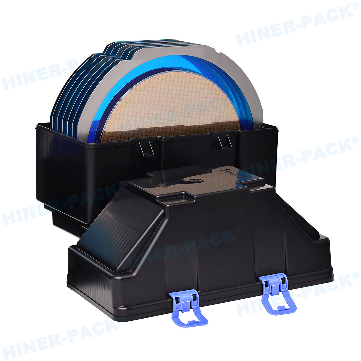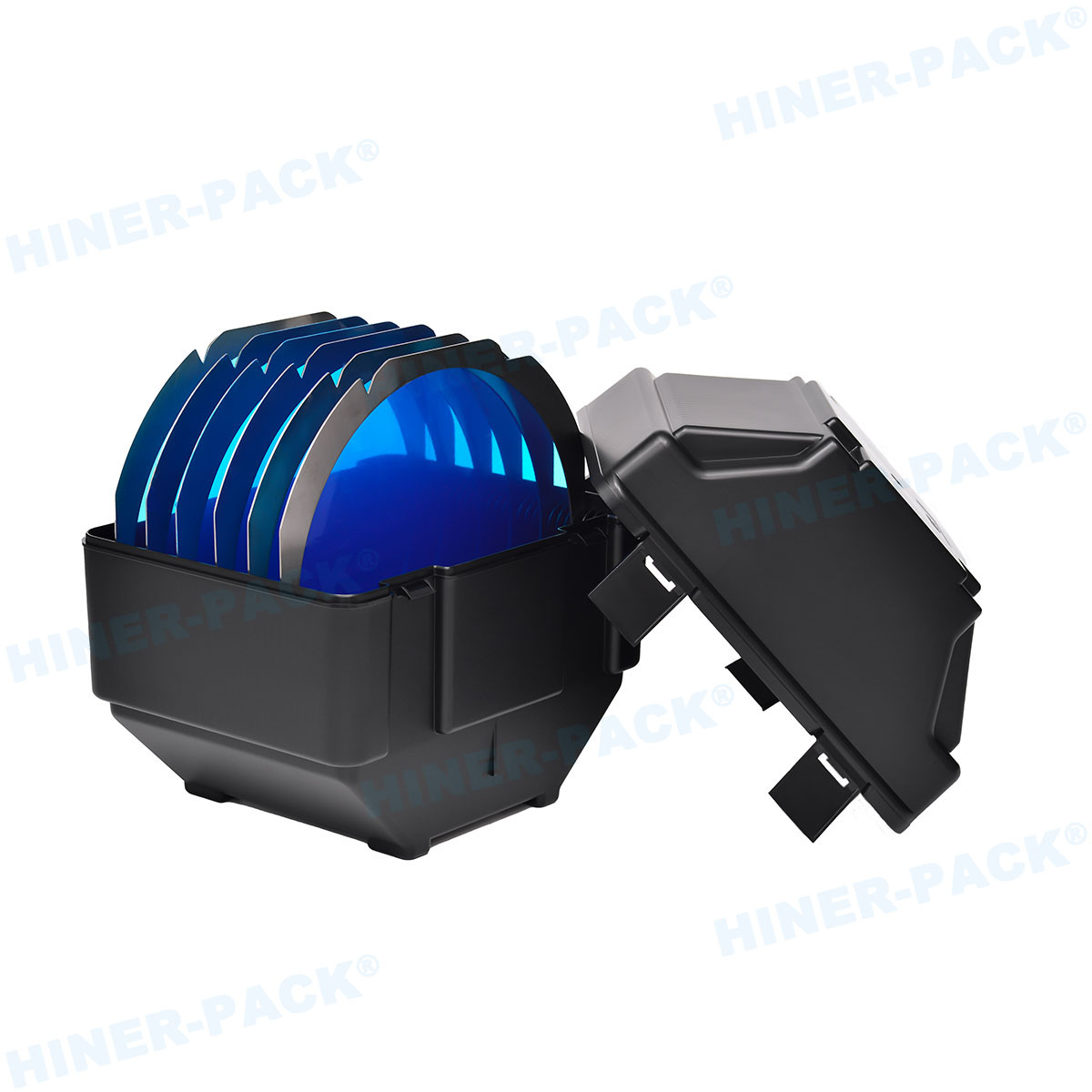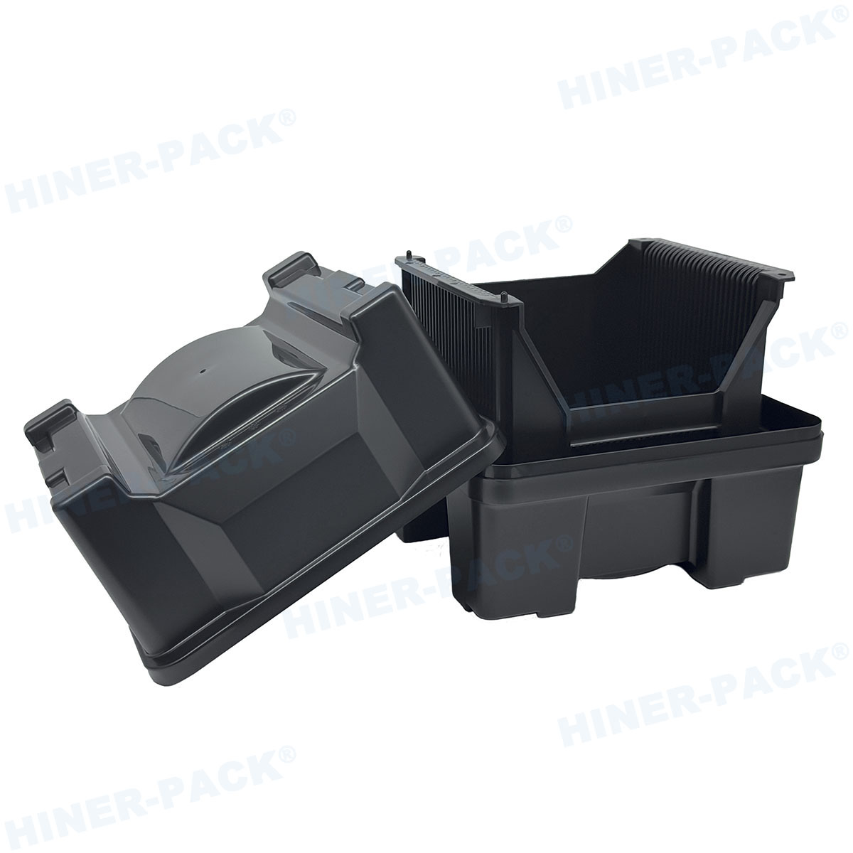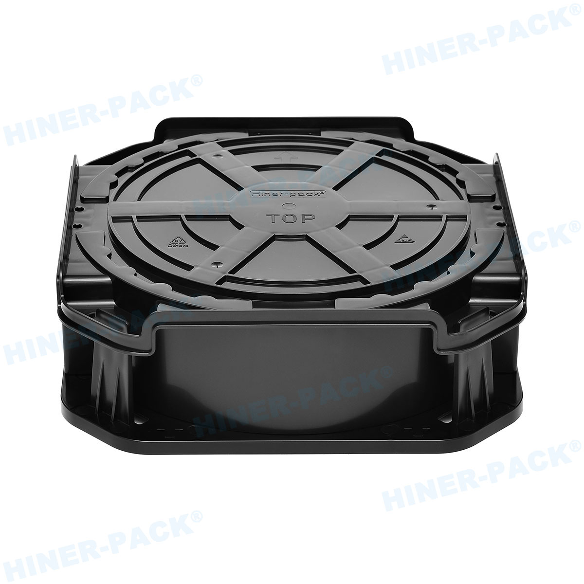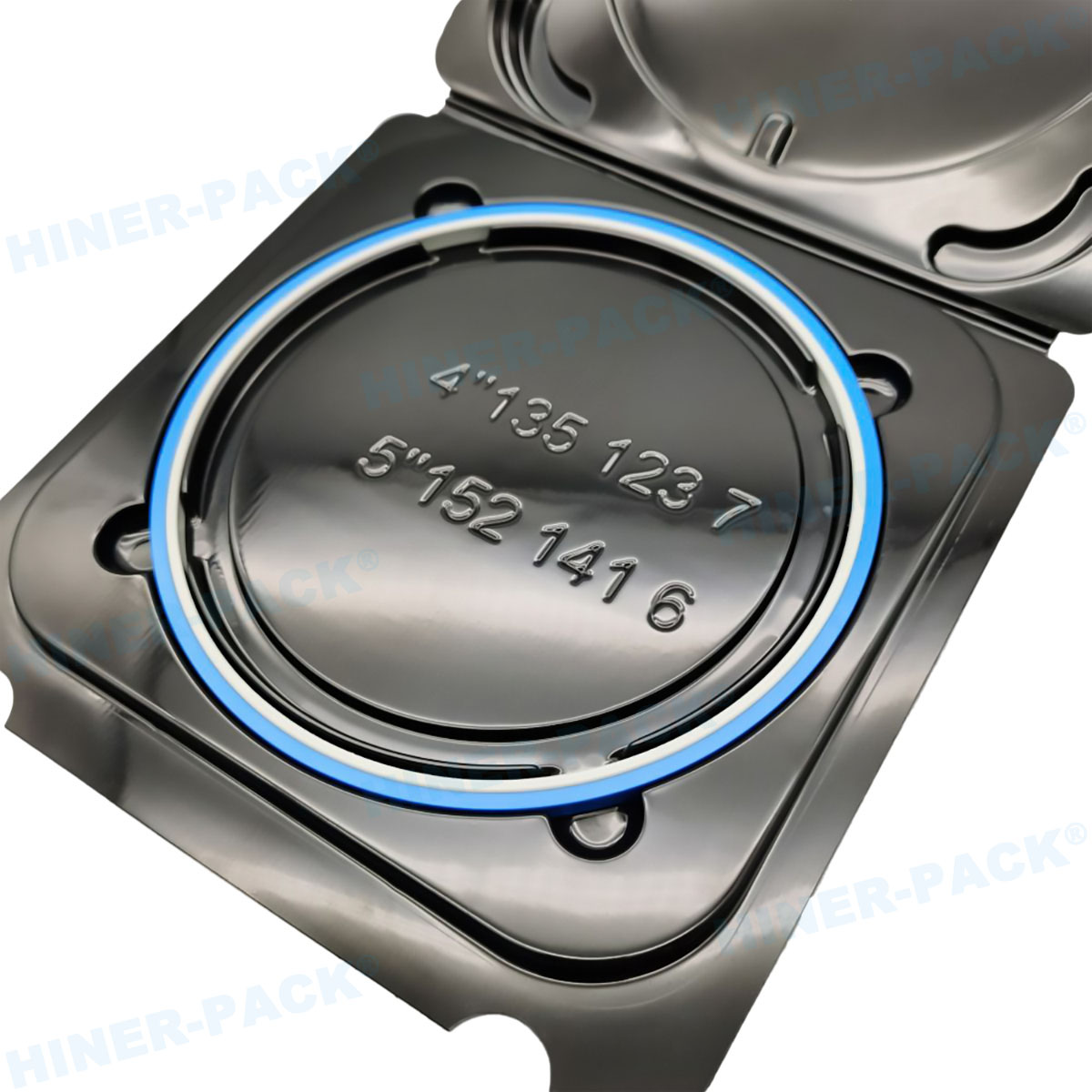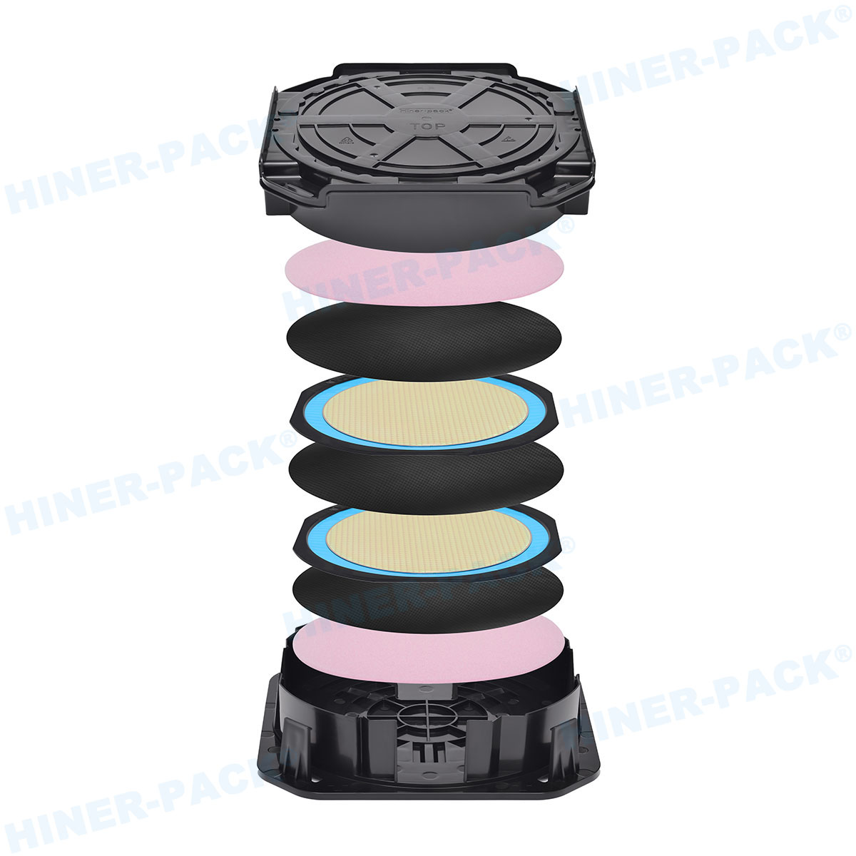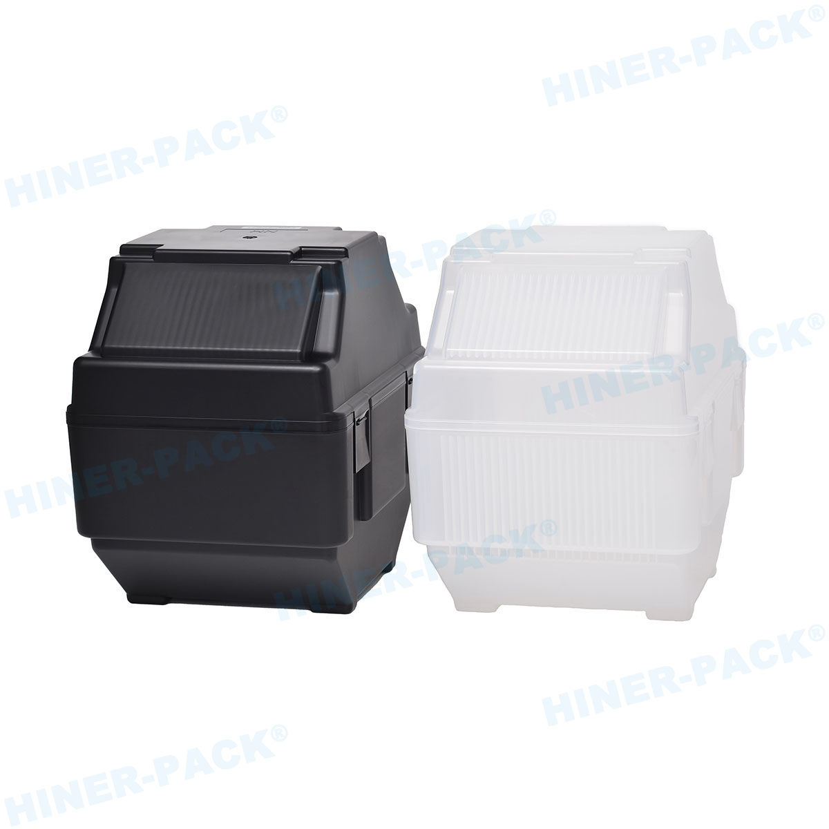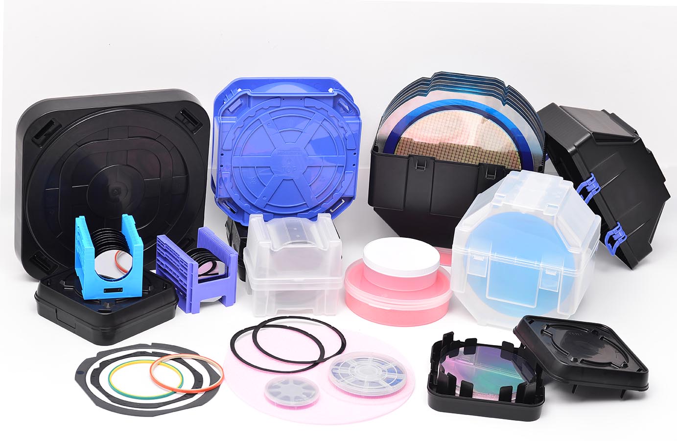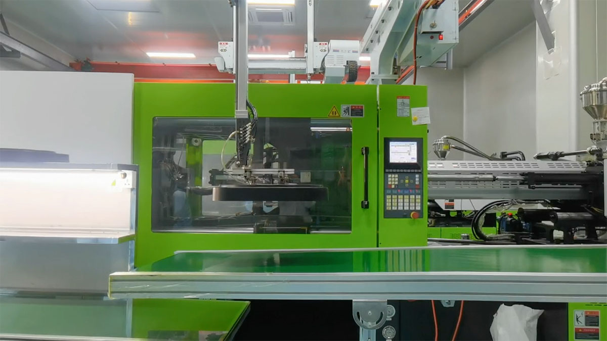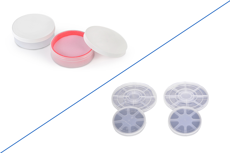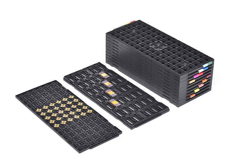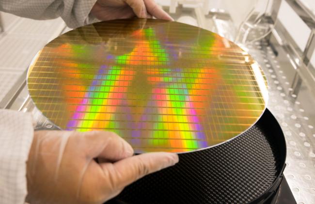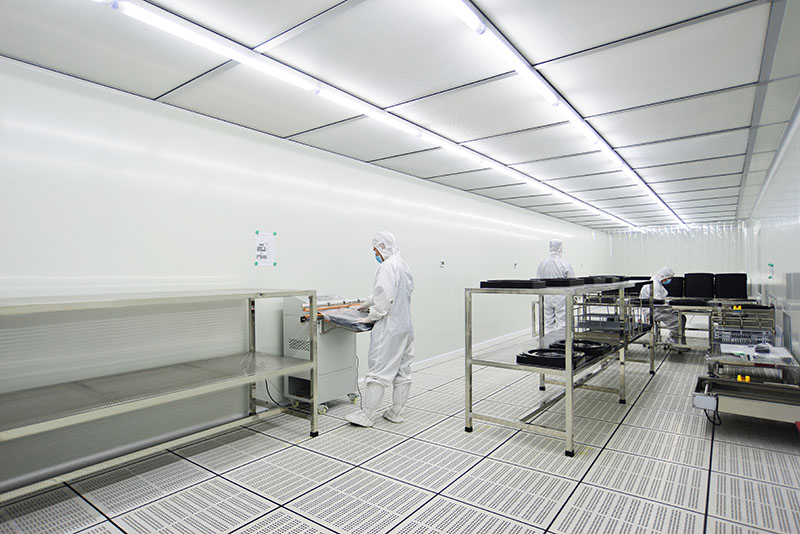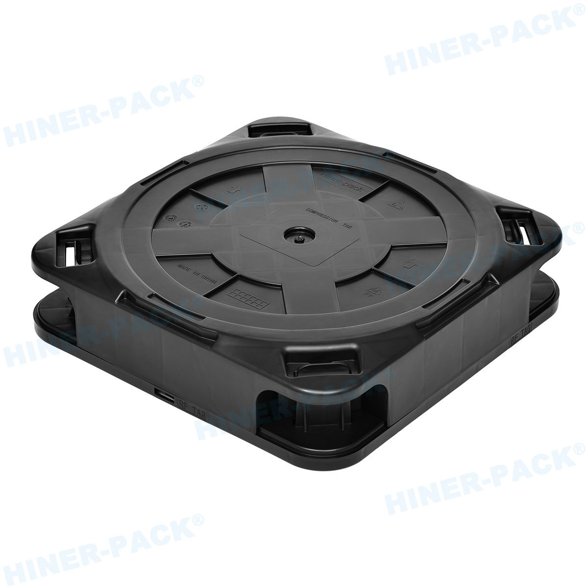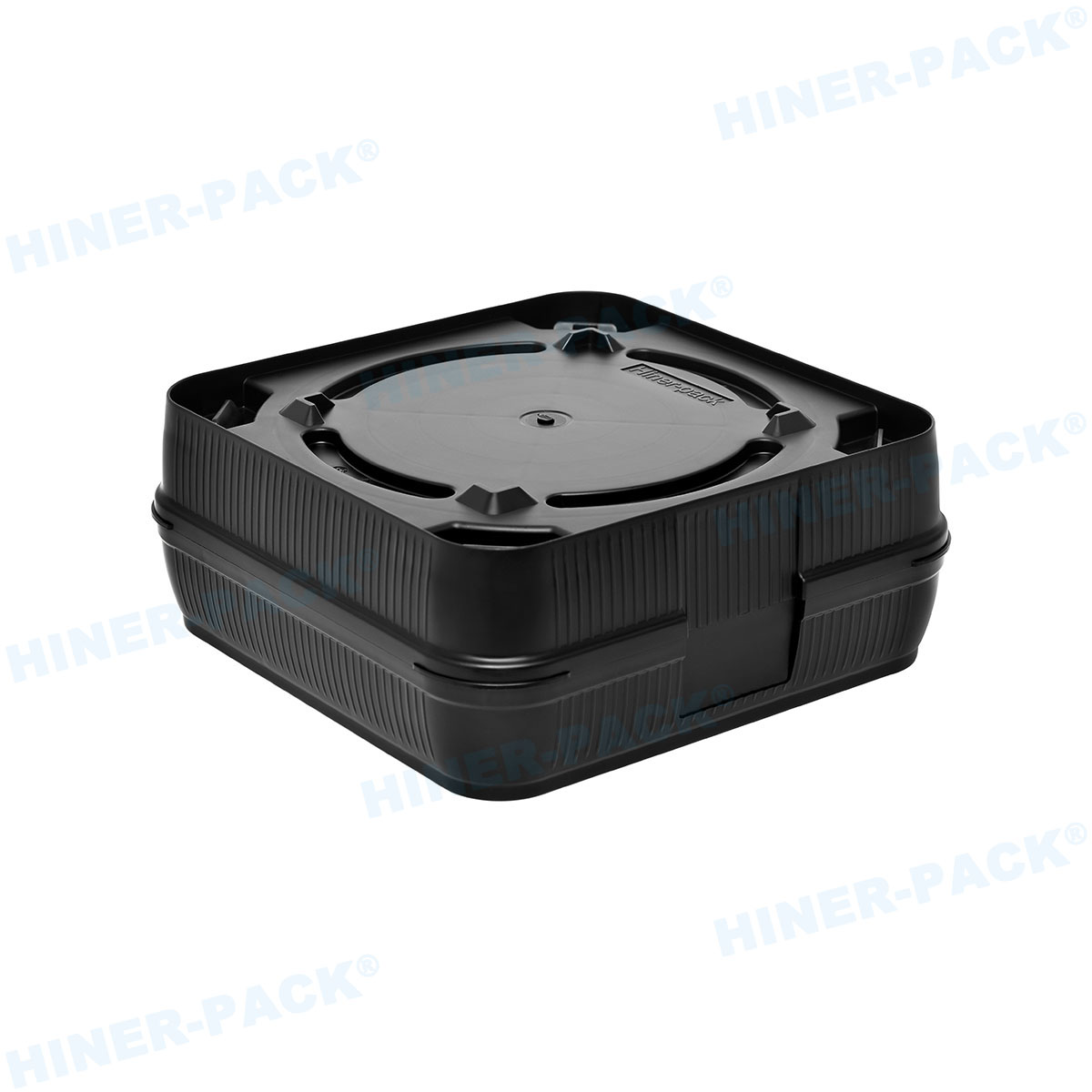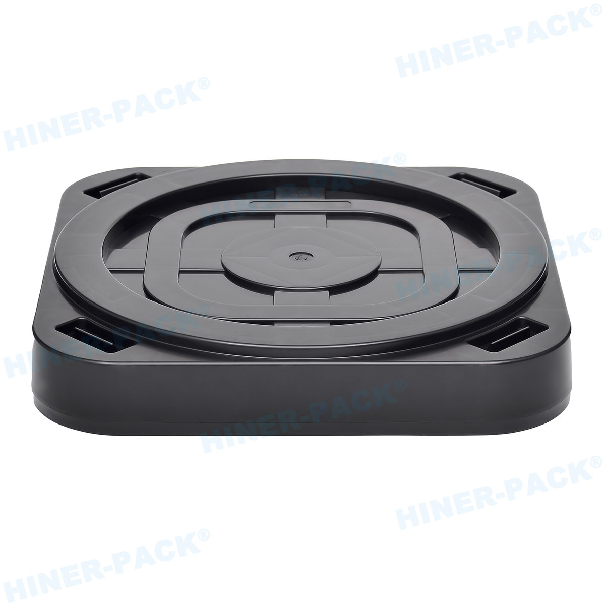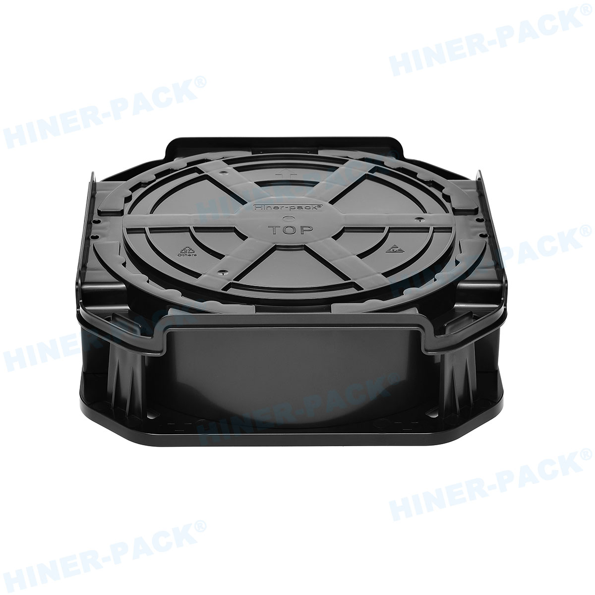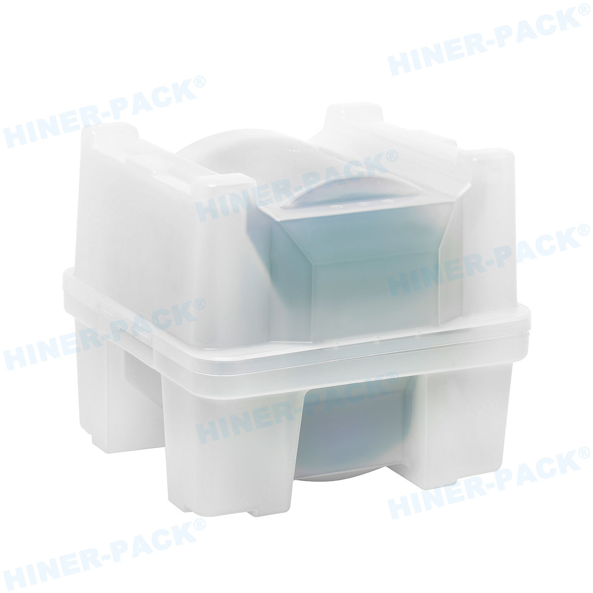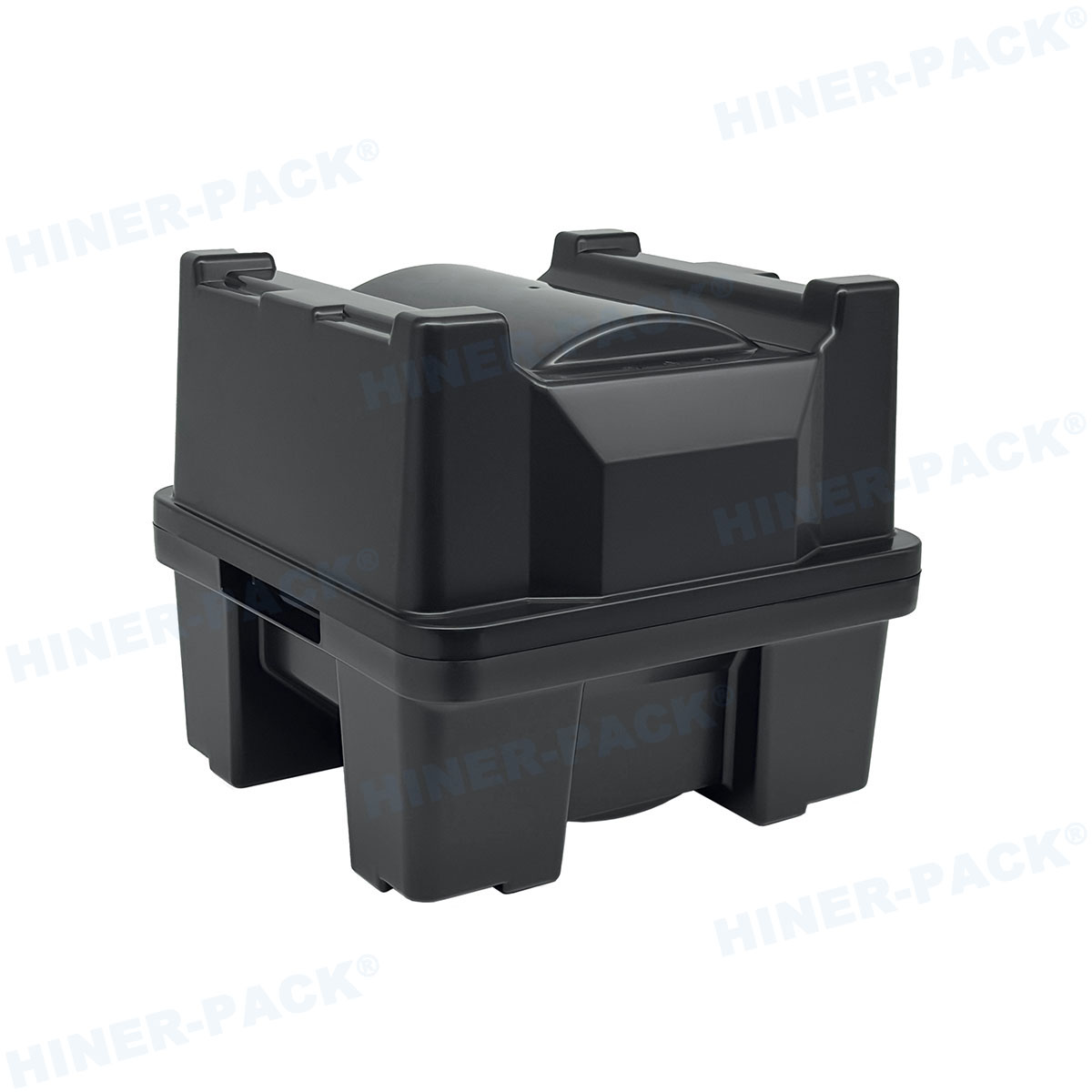
FOSB Wafer Shippers: Engineering Integrity for 300mm Semiconductor Logistics
In the high-stakes environment of semiconductor manufacturing, the physical
transport and storage of 300mm silicon wafers between the wafer fab and t ...
2026-07-09
View More